- 您现在的位置:买卖IC网 > PDF目录16847 > AD9513/PCBZ (Analog Devices Inc)BOARD EVAL FOR AD9513 PDF资料下载
参数资料
| 型号: | AD9513/PCBZ |
| 厂商: | Analog Devices Inc |
| 文件页数: | 10/28页 |
| 文件大小: | 0K |
| 描述: | BOARD EVAL FOR AD9513 |
| 设计资源: | AD9513/14/15 Eval Brd Schematics AD9513/14/15 Gerber Files AD9513 Eval Brd BOM |
| 标准包装: | 1 |
| 主要目的: | 计时,时钟分配 |
| 已用 IC / 零件: | AD9513 |
| 已供物品: | 板 |
| 相关产品: | AD9513BCPZ-ND - IC CLOCK DIST 3OUT PLL 32LFCSP AD9513BCPZ-REEL7-ND - IC CLOCK DIST 3OUT PLL 32LFCSP |
第1页第2页第3页第4页第5页第6页第7页第8页第9页当前第10页第11页第12页第13页第14页第15页第16页第17页第18页第19页第20页第21页第22页第23页第24页第25页第26页第27页第28页
AD9513
Rev. 0 | Page 18 of 28
Synchronization is initiated by pulling the SYNCB pin low for a
minimum of 5 ns. The input clock does not have to be present
at the time the command is issued. The synchronization occurs
after four input clock cycles.
The synchronization applies to clock outputs
that are not turned OFF
where the divider is not divide = 1 (divider bypassed)
An output with its divider set to divide = 1 (divider bypassed)
is always synchronized with the input clock, with a propagation
delay.
The SYNCB pin must be pulled up for normal operation. Do
not let the SYNCB pin float.
RSET RESISTOR
The internal bias currents of the AD9513 are set by the
RSET resistor. This resistor should be as close as possible to
the value given as a condition in the Specifications section
(RSET = 4.12 kΩ). This is a standard 1% resistor value and should
be readily obtainable. The bias currents set by this resistor
determine the logic levels and operating conditions of the
internal blocks of the AD9513. The performance figures given
in the Specifications section assume that this resistor value is
used for RSET.
VREF
The VREF pin provides a voltage level of VS. This voltage is
one of the four logic levels used by the setup pins (S0 to S10).
These pins set the operation of the AD9513. The VREF pin
provides sufficient drive capability to drive as many of the setup
pins as necessary, up to all on a single part. The VREF pin
should be used for no other purpose.
SETUP CONFIGURATION
The specific operation of the AD9513 is set by the logic levels
applied to the setup pins (S10 to S0). These pins use four-state
logic. The logic levels used are VS and GND, plus VS and
VS. The VS level is provided by the internal self-biasing on
each of the setup pins (S10 to S0). This is the level seen by a
setup pin that is left not connected (NC). The VS level is
provided by the VREF pin. All setup pins requiring the VS
level must be tied to the VREF pin.
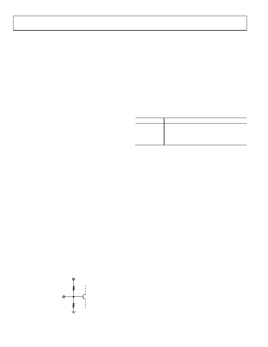
SETUP PIN
S0 TO S10
60k
30k
VS
05595
-0
23
Figure 23. Setup Pin (S0 to S10) Equivalent Circuit
The AD9513 operation is determined by the combination of
logic levels present at the setup pins. The setup configurations
logic levels are referred to as 0, , , and 1. These numbers
represent the fraction of the VS voltage that defines the logic
levels. See the setup pin thresholds in Table 6.
The meaning of some of the pin settings is changed by the
settings of other pins. For example, S0 determines whether S3,
and S4 sets OUT2 delay (S0 ≠ 0) or OUT2 phase (S0 = 0).
S2 indicates which outputs are in use, as shown in Table 10. This
allows the same pins (S5 and S6, S7 and S8) to determine the
settings for two different outputs, depending on which outputs
are in use.
Table 10. S2 Indicates Which Outputs Are in Use
S2
Outputs
0
OUT2 Off
1/3
All Outputs On
2/3
OUT0 Off
1
OUT1 Off
The fine delay values set by S3 and S4 (when the delay is being
used, S0 ≠ 0) are fractions of the full-scale delay. Note that the
longest setting is 15/16 of full scale. The full-scale delay times
are given in Table 3. To determine the actual delay, take the
fraction corresponding to the fine delay setting and multiply by
the full-scale value set by Table 3 corresponding to the S0 value
and add the LVDS or CMOS propagation delay time (see Table 3).
The full-scale delay times shown in Table 11, and referred to
elsewhere, are nominal time values.
The value at S2 also determines whether S5 and S6 set OUT2
divide (S2 ≠ 0) or OUT1 phase (S2 = 0). In addition, S2
determines whether S7 and S8 set OUT1 divide (S2 ≠ 1) or
OUT2 phase (S2 = 1 and S0 ≠ 0). In addition, the value of S2
determines whether S9 and S10 set OUT0 divide (S2 ≠ 2/3) or
OUT2 divide (S2 = 2/3).
相关PDF资料 |
PDF描述 |
|---|---|
| AD9516-1/PCBZ | BOARD EVALUATION FOR AD9516-1 |
| MAX876AESA+T | IC VREF SERIES PREC 10V 8-SOIC |
| 35PX22MEFC5X11 | CAP ALUM 22UF 35V 20% RADIAL |
| GCC07DRYS-S734 | CONN EDGECARD 14POS DIP .100 SLD |
| MAX6177BASA+ | IC VREF SERIES PREC 3.3V 8-SOIC |
相关代理商/技术参数 |
参数描述 |
|---|---|
| AD9514 | 制造商:AD 制造商全称:Analog Devices 功能描述:1.6 GHz Clock Distribution IC, Dividers, Delay Adjust, Three Outputs |
| AD9514/PCB | 制造商:Analog Devices 功能描述:CLOCK DISTRIBUTION - Bulk |
| AD9514/PCBZ | 功能描述:BOARD EVAL CLOCK 3CH AD9514 RoHS:是 类别:编程器,开发系统 >> 评估演示板和套件 系列:- 标准包装:1 系列:- 主要目的:电信,线路接口单元(LIU) 嵌入式:- 已用 IC / 零件:IDT82V2081 主要属性:T1/J1/E1 LIU 次要属性:- 已供物品:板,电源,线缆,CD 其它名称:82EBV2081 |
| AD9514BCPZ | 功能描述:IC CLOCK DIST 3OUT PLL 32LFCSP RoHS:是 类别:集成电路 (IC) >> 时钟/计时 - 时钟发生器,PLL,频率合成器 系列:- 标准包装:2,000 系列:- 类型:PLL 频率合成器 PLL:是 输入:晶体 输出:时钟 电路数:1 比率 - 输入:输出:1:1 差分 - 输入:输出:无/无 频率 - 最大:1GHz 除法器/乘法器:是/无 电源电压:4.5 V ~ 5.5 V 工作温度:-20°C ~ 85°C 安装类型:表面贴装 封装/外壳:16-LSSOP(0.175",4.40mm 宽) 供应商设备封装:16-SSOP 包装:带卷 (TR) 其它名称:NJW1504V-TE1-NDNJW1504V-TE1TR |
| AD9514BCPZ-REEL7 | 功能描述:IC CLOCK DIST 3OUT PLL 32LFCSP RoHS:是 类别:集成电路 (IC) >> 时钟/计时 - 时钟发生器,PLL,频率合成器 系列:- 标准包装:1,000 系列:Precision Edge® 类型:时钟/频率合成器 PLL:无 输入:CML,PECL 输出:CML 电路数:1 比率 - 输入:输出:2:1 差分 - 输入:输出:是/是 频率 - 最大:10.7GHz 除法器/乘法器:无/无 电源电压:2.375 V ~ 3.6 V 工作温度:-40°C ~ 85°C 安装类型:表面贴装 封装/外壳:16-VFQFN 裸露焊盘,16-MLF? 供应商设备封装:16-MLF?(3x3) 包装:带卷 (TR) 其它名称:SY58052UMGTRSY58052UMGTR-ND |
发布紧急采购,3分钟左右您将得到回复。