- 您现在的位置:买卖IC网 > PDF目录16847 > AD9516-1/PCBZ (Analog Devices Inc)BOARD EVALUATION FOR AD9516-1 PDF资料下载
参数资料
| 型号: | AD9516-1/PCBZ |
| 厂商: | Analog Devices Inc |
| 文件页数: | 1/80页 |
| 文件大小: | 0K |
| 描述: | BOARD EVALUATION FOR AD9516-1 |
| 产品培训模块: | Active Filter Design Tools |
| 设计资源: | AD9516 Eval Brd Schematic AD9516 Gerber Files AD9516-1 BOM |
| 标准包装: | 1 |
| 主要目的: | 计时,时钟发生器 |
| 嵌入式: | 否 |
| 已用 IC / 零件: | AD9516-1 |
| 主要属性: | 2 输入,14 输出,2.5GHz VCO |
| 次要属性: | CMOS、LVDS、LVPECL 输出逻辑,ADIsimCLK&trade 图形用户界面 |
| 已供物品: | 板,线缆,电源 |
| 产品目录页面: | 776 (CN2011-ZH PDF) |
| 相关产品: | AD9516-1BCPZ-REEL7-ND - IC CLOCK GEN 2.5GHZ VCO 64-LFCSP AD9516-1BCPZ-ND - IC CLOCK GEN 2.5GHZ VCO 64-LFCSP |
当前第1页第2页第3页第4页第5页第6页第7页第8页第9页第10页第11页第12页第13页第14页第15页第16页第17页第18页第19页第20页第21页第22页第23页第24页第25页第26页第27页第28页第29页第30页第31页第32页第33页第34页第35页第36页第37页第38页第39页第40页第41页第42页第43页第44页第45页第46页第47页第48页第49页第50页第51页第52页第53页第54页第55页第56页第57页第58页第59页第60页第61页第62页第63页第64页第65页第66页第67页第68页第69页第70页第71页第72页第73页第74页第75页第76页第77页第78页第79页第80页
14-Output Clock Generator with
Integrated 2.5 GHz VCO
Data Sheet
Rev. C
Information furnished by Analog Devices is believed to be accurate and reliable. However, no
responsibilityisassumedbyAnalogDevicesforitsuse,norforanyinfringementsofpatentsorother
rightsofthirdpartiesthatmayresultfromitsuse.Specificationssubjecttochangewithoutnotice.No
license is granted by implication or otherwise under any patent or patent rights of Analog Devices.
Trademarksandregisteredtrademarksarethepropertyoftheirrespectiveowners.
One Technology Way, P.O. Box 9106, Norwood, MA 02062-9106, U.S.A.
Tel: 781.329.4700
2007–2013 Analog Devices, Inc. All rights reserved.
FEATURES
Low phase noise, phase-locked loop (PLL)
On-chip VCO tunes from 2.30 GHz to 2.65 GHz
External VCO/VCXO to 2.4 GHz optional
1 differential or 2 single-ended reference inputs
Reference monitoring capability
Automatic revertive and manual reference
switchover/holdover modes
Accepts LVPECL, LVDS, or CMOS references to 250 MHz
Programmable delays in path to PFD
Digital or analog lock detect, selectable
6 pairs of 1.6 GHz LVPECL outputs
Each output pair shares a 1-to-32 divider with coarse
phase delay
Additive output jitter: 225 fs rms
Channel-to-channel skew paired outputs of <10 ps
4 pairs of 800 MHz LVDS clock outputs
Each output pair shares two cascaded 1-to-32 dividers
with coarse phase delay
Additive output jitter: 275 fs rms
Fine delay adjust (Δt) on each LVDS output
Each LVDS output can be reconfigured as two 250 MHz
CMOS outputs
Automatic synchronization of all outputs on power-up
Manual output synchronization available
64-lead LFCSP
APPLICATIONS
Low jitter, low phase noise clock distribution
10/40/100 Gb/sec networking line cards, including SONET,
Synchronous Ethernet, OTU2/3/4
Forward error correction (G.710)
Clocking high speed ADCs, DACs, DDSs, DDCs, DUCs, MxFEs
High performance wireless transceivers
ATE and high performance instrumentation
GENERAL DESCRIPTION
The AD9516-11 provides a multi-output clock distribution
function with subpicosecond jitter performance, along with an on-
chip PLL and VCO. The on-chip VCO tunes from 2.30 GHz to
2.65 GHz. Optionally, an external VCO/VCXO of up to 2.4 GHz
can be used.
The AD9516-1 emphasizes low jitter and phase noise to
maximize data converter performance, and it can benefit other
applications with demanding phase noise and jitter requirements.
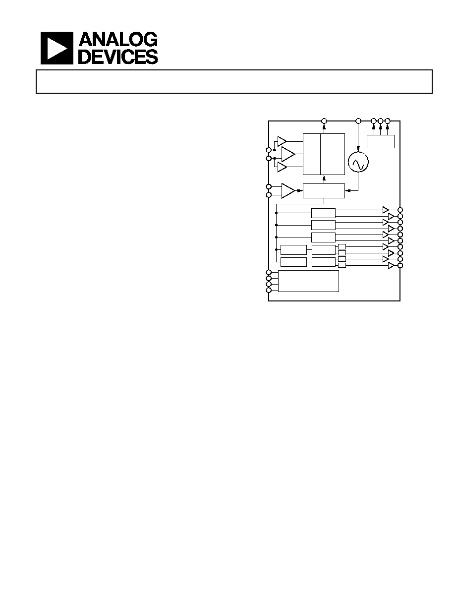
FUNCTIONAL BLOCK DIAGRAM
REFIN
REF1
REF2
CLK
LF
SW
IT
C
H
O
VER
AND
M
O
NI
T
O
R
PL
L
DIVIDER
AND MUXs
CP
VCO
STATUS
MONITOR
LVPECL
LVDS/CMOS
SERIAL CONTROL PORT
AND
DIGITAL LOGIC
AD9516-1
OUT0
OUT1
OUT2
OUT3
OUT4
OUT5
OUT6
OUT7
OUT8
OUT9
DIV/Φ
Δt
06420-
001
Figure 1.
The AD9516-1 features six LVPECL outputs (in three pairs) and
four LVDS outputs (in two pairs). Each LVDS output can be
reconfigured as two CMOS outputs. The LVPECL outputs
operate to 1.6 GHz, the LVDS outputs operate to 800 MHz, and
the CMOS outputs operate to 250 MHz.
Each pair of outputs has dividers that allow both the divide ratio
and coarse delay (or phase) to be set. The range of division for
the LVPECL outputs is 1 to 32. The LVDS/CMOS outputs allow
a range of divisions up to a maximum of 1024.
The AD9516-1 is available in a 64-lead LFCSP and can be
operated from a single 3.3 V supply. An external VCO, which
requires an extended voltage range, can be accommodated by
connecting the charge pump supply (VCP) to 5 V. A separate
LVPECL power supply can be from 2.5 V to 3.3 V (nominal).
The AD9516-1 is specified for operation over the industrial
range of 40°C to +85°C.
1
AD9516 is used throughout to refer to all the members of the AD9516 family.
However, when AD9516-1 is used, it refers to that specific member of the
AD9516 family.
相关PDF资料 |
PDF描述 |
|---|---|
| MAX876AESA+T | IC VREF SERIES PREC 10V 8-SOIC |
| 35PX22MEFC5X11 | CAP ALUM 22UF 35V 20% RADIAL |
| GCC07DRYS-S734 | CONN EDGECARD 14POS DIP .100 SLD |
| MAX6177BASA+ | IC VREF SERIES PREC 3.3V 8-SOIC |
| AD9516-4/PCBZ | BOARD EVAL FOR AD9516-4 1.8GHZ |
相关代理商/技术参数 |
参数描述 |
|---|---|
| AD9516-1XCPZ | 制造商:Analog Devices 功能描述:14-CHANNEL CLOCK GENERATOR WITH INTEGRATED 2.8 GHZ VCO - Bulk |
| AD9516-2 | 制造商:AD 制造商全称:Analog Devices 功能描述:14-Output Clock Generator with Integrated 2.2 GHz VCO |
| AD9516-2/PCBZ | 功能描述:BOARD EVAL FOR AD9516-2 2.2GHZ RoHS:是 类别:编程器,开发系统 >> 评估演示板和套件 系列:- 标准包装:1 系列:- 主要目的:电信,线路接口单元(LIU) 嵌入式:- 已用 IC / 零件:IDT82V2081 主要属性:T1/J1/E1 LIU 次要属性:- 已供物品:板,电源,线缆,CD 其它名称:82EBV2081 |
| AD9516-2BCPZ | 功能描述:IC CLOCK PLL/VCO 2.2GHZ 64LFCSP RoHS:是 类别:集成电路 (IC) >> 时钟/计时 - 时钟发生器,PLL,频率合成器 系列:- 标准包装:2,000 系列:- 类型:PLL 时钟发生器 PLL:带旁路 输入:LVCMOS,LVPECL 输出:LVCMOS 电路数:1 比率 - 输入:输出:2:11 差分 - 输入:输出:是/无 频率 - 最大:240MHz 除法器/乘法器:是/无 电源电压:3.135 V ~ 3.465 V 工作温度:0°C ~ 70°C 安装类型:表面贴装 封装/外壳:32-LQFP 供应商设备封装:32-TQFP(7x7) 包装:带卷 (TR) |
| AD9516-2BCPZ-REEL7 | 功能描述:IC CLOCK PLL/VCO 2.2GHZ 64LFCSP RoHS:是 类别:集成电路 (IC) >> 时钟/计时 - 时钟发生器,PLL,频率合成器 系列:- 标准包装:2,000 系列:- 类型:PLL 时钟发生器 PLL:带旁路 输入:LVCMOS,LVPECL 输出:LVCMOS 电路数:1 比率 - 输入:输出:2:11 差分 - 输入:输出:是/无 频率 - 最大:240MHz 除法器/乘法器:是/无 电源电压:3.135 V ~ 3.465 V 工作温度:0°C ~ 70°C 安装类型:表面贴装 封装/外壳:32-LQFP 供应商设备封装:32-TQFP(7x7) 包装:带卷 (TR) |
发布紧急采购,3分钟左右您将得到回复。