- 您现在的位置:买卖IC网 > PDF目录16847 > AD9516-1/PCBZ (Analog Devices Inc)BOARD EVALUATION FOR AD9516-1 PDF资料下载
参数资料
| 型号: | AD9516-1/PCBZ |
| 厂商: | Analog Devices Inc |
| 文件页数: | 36/80页 |
| 文件大小: | 0K |
| 描述: | BOARD EVALUATION FOR AD9516-1 |
| 产品培训模块: | Active Filter Design Tools |
| 设计资源: | AD9516 Eval Brd Schematic AD9516 Gerber Files AD9516-1 BOM |
| 标准包装: | 1 |
| 主要目的: | 计时,时钟发生器 |
| 嵌入式: | 否 |
| 已用 IC / 零件: | AD9516-1 |
| 主要属性: | 2 输入,14 输出,2.5GHz VCO |
| 次要属性: | CMOS、LVDS、LVPECL 输出逻辑,ADIsimCLK&trade 图形用户界面 |
| 已供物品: | 板,线缆,电源 |
| 产品目录页面: | 776 (CN2011-ZH PDF) |
| 相关产品: | AD9516-1BCPZ-REEL7-ND - IC CLOCK GEN 2.5GHZ VCO 64-LFCSP AD9516-1BCPZ-ND - IC CLOCK GEN 2.5GHZ VCO 64-LFCSP |
第1页第2页第3页第4页第5页第6页第7页第8页第9页第10页第11页第12页第13页第14页第15页第16页第17页第18页第19页第20页第21页第22页第23页第24页第25页第26页第27页第28页第29页第30页第31页第32页第33页第34页第35页当前第36页第37页第38页第39页第40页第41页第42页第43页第44页第45页第46页第47页第48页第49页第50页第51页第52页第53页第54页第55页第56页第57页第58页第59页第60页第61页第62页第63页第64页第65页第66页第67页第68页第69页第70页第71页第72页第73页第74页第75页第76页第77页第78页第79页第80页
Data Sheet
AD9516-1
Rev. C | Page 41 of 80
To connect the LVPECL outputs directly to the internal VCO or
CLK, the VCO divider must be selected as the source to the
distribution section, even if no channel uses it.
Either the internal VCO or the CLK can be selected as the
source for the direct to output routing.
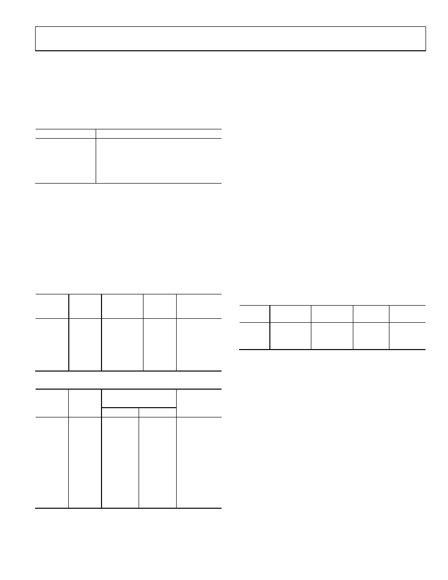
Table 31. Settings for Routing VCO Divider Input Directly
to LVPECL Outputs
Register Setting
Selection
0x1E1[1:0] = 00b
CLK is the source; VCO divider selected
0x1E1[1:0] = 10b
VCO is the source; VCO divider selected
0x192[1] = 1b
Direct to output OUT0, OUT1
0x195[1] = 1b
Direct to output OUT2, OUT3
0x198[1] = 1b
Direct to output OUT4, OUT5
Clock Frequency Division
The total frequency division is a combination of the VCO
divider (when used) and the channel divider. When the VCO
divider is used, the total division from the VCO or CLK to the
output is the product of the VCO divider (2, 3, 4, 5, 6) and the
division of the channel divider. Table 32 and Table 33 indicate
how the frequency division for a channel is set. For the LVPECL
outputs, there is only one divider per channel. For the LVDS/
CMOS outputs, there are two dividers (X.1, X.2) cascaded
per channel.
Table 32. Frequency Division for Divider 0 to Divider 2
CLK
or VCO
Selected
VCO
Divider
Channel
Divider
Direct to
Output
Frequency
Division
CLK/VCO
2 to 6
1 (bypassed)
Yes
1
CLK/VCO
2 to 6
1 (bypassed)
No
(2 to 6) × (1)
CLK/VCO
2 to 6
2 to 32
No
(2 to 6) ×
(2 to 32)
CLK
Not used
1 (bypassed)
No
1
CLK
Not used
2 to 32
No
2 to 32
Table 33. Frequency Division for Divider 3 and Divider 4
CLK
or VCO
Selected
VCO
Divider
Channel Divider
Frequency
Division
X.1
X.2
CLK/VCO
2 to 6
1
(bypassed)
1
(bypassed)
(2 to 6) ×
(1) × (1)
CLK/VCO
2 to 6
2 to 32
1
(bypassed)
(2 to 6) ×
(2 to 32) × (1)
CLK/VCO
2 to 6
2 to 32
(2 to 6) ×
(2 to 32) ×
(2 to 32)
CLK
Not used
1
CLK
Not used
2 to 32
1
(2 to 32) × (1)
CLK
Not used
2 to 32
2 to 32 ×
(2 to 32)
The channel dividers feeding the LVPECL output drivers
contain one 2-to-32 frequency divider. This divider provides for
division by 2 to 32. Division by 1 is accomplished by bypassing
the divider. The dividers also provide for a programmable duty
cycle, with optional duty-cycle correction when the divide ratio
is odd. A phase offset or delay in increments of the input clock
cycle is selectable. The channel dividers operate with a signal at
their inputs up to 1600 MHz. The features and settings of the
dividers are selected by programming the appropriate setup
and control registers (see Table 52 through Table 62).
VCO Divider
The VCO divider provides frequency division between the
internal VCO or the external CLK input and the clock
distribution channel dividers. The VCO divider can be set
to divide by 2, 3, 4, 5, or 6 (see Table 60, Register 0x1E0[2:0]).
Channel Dividers—LVPECL Outputs
Each pair of LVPECL outputs is driven by a channel divider.
There are three channel dividers (0, 1, and 2) driving a total of
six LVPECL outputs (OUT0 to OUT5). Table 34 lists the register
locations used for setting the division and other functions of
these dividers. The division is set by the values of M and N. The
divider can be bypassed (equivalent to divide-by-1, divider circuit
is powered down) by setting the bypass bit. The duty-cycle
correction can be enabled or disabled according to the setting of
the DCCOFF bits.
Table 34. Setting DX for Divider 0, Divider 1, and Divider 21
Divider
Low Cycles
M
High Cycles
N
Bypass
DCCOFF
0
0x190[7:4]
0x190[3:0]
0x191[7]
0x192[0]
1
0x193[7:4]
0x193[3:0]
0x194[7]
0x195[0]
2
0x196[7:4]
0x196[3:0]
0x197[7]
0x198[0]
1
Note that the value stored in the register = # of cycles minus 1.
Channel Frequency Division (0, 1, and 2)
For each channel (where the channel number is x: 0, 1, or 2),
the frequency division, DX, is set by the values of M and N
(four bits each, representing Decimal 0 to Decimal 15), where
Number of Low Cycles = M + 1
Number of High Cycles = N + 1
The cycles are cycles of the clock signal currently routed to the
input of the channel dividers (VCO divider out or CLK).
When a divider is bypassed, DX = 1.
Otherwise, DX = (N + 1) + (M + 1) = N + M + 2. This allows
each channel divider to divide by any integer from 2 to 32.
相关PDF资料 |
PDF描述 |
|---|---|
| MAX876AESA+T | IC VREF SERIES PREC 10V 8-SOIC |
| 35PX22MEFC5X11 | CAP ALUM 22UF 35V 20% RADIAL |
| GCC07DRYS-S734 | CONN EDGECARD 14POS DIP .100 SLD |
| MAX6177BASA+ | IC VREF SERIES PREC 3.3V 8-SOIC |
| AD9516-4/PCBZ | BOARD EVAL FOR AD9516-4 1.8GHZ |
相关代理商/技术参数 |
参数描述 |
|---|---|
| AD9516-1XCPZ | 制造商:Analog Devices 功能描述:14-CHANNEL CLOCK GENERATOR WITH INTEGRATED 2.8 GHZ VCO - Bulk |
| AD9516-2 | 制造商:AD 制造商全称:Analog Devices 功能描述:14-Output Clock Generator with Integrated 2.2 GHz VCO |
| AD9516-2/PCBZ | 功能描述:BOARD EVAL FOR AD9516-2 2.2GHZ RoHS:是 类别:编程器,开发系统 >> 评估演示板和套件 系列:- 标准包装:1 系列:- 主要目的:电信,线路接口单元(LIU) 嵌入式:- 已用 IC / 零件:IDT82V2081 主要属性:T1/J1/E1 LIU 次要属性:- 已供物品:板,电源,线缆,CD 其它名称:82EBV2081 |
| AD9516-2BCPZ | 功能描述:IC CLOCK PLL/VCO 2.2GHZ 64LFCSP RoHS:是 类别:集成电路 (IC) >> 时钟/计时 - 时钟发生器,PLL,频率合成器 系列:- 标准包装:2,000 系列:- 类型:PLL 时钟发生器 PLL:带旁路 输入:LVCMOS,LVPECL 输出:LVCMOS 电路数:1 比率 - 输入:输出:2:11 差分 - 输入:输出:是/无 频率 - 最大:240MHz 除法器/乘法器:是/无 电源电压:3.135 V ~ 3.465 V 工作温度:0°C ~ 70°C 安装类型:表面贴装 封装/外壳:32-LQFP 供应商设备封装:32-TQFP(7x7) 包装:带卷 (TR) |
| AD9516-2BCPZ-REEL7 | 功能描述:IC CLOCK PLL/VCO 2.2GHZ 64LFCSP RoHS:是 类别:集成电路 (IC) >> 时钟/计时 - 时钟发生器,PLL,频率合成器 系列:- 标准包装:2,000 系列:- 类型:PLL 时钟发生器 PLL:带旁路 输入:LVCMOS,LVPECL 输出:LVCMOS 电路数:1 比率 - 输入:输出:2:11 差分 - 输入:输出:是/无 频率 - 最大:240MHz 除法器/乘法器:是/无 电源电压:3.135 V ~ 3.465 V 工作温度:0°C ~ 70°C 安装类型:表面贴装 封装/外壳:32-LQFP 供应商设备封装:32-TQFP(7x7) 包装:带卷 (TR) |
发布紧急采购,3分钟左右您将得到回复。