- 您现在的位置:买卖IC网 > PDF目录16847 > AD9516-1/PCBZ (Analog Devices Inc)BOARD EVALUATION FOR AD9516-1 PDF资料下载
参数资料
| 型号: | AD9516-1/PCBZ |
| 厂商: | Analog Devices Inc |
| 文件页数: | 76/80页 |
| 文件大小: | 0K |
| 描述: | BOARD EVALUATION FOR AD9516-1 |
| 产品培训模块: | Active Filter Design Tools |
| 设计资源: | AD9516 Eval Brd Schematic AD9516 Gerber Files AD9516-1 BOM |
| 标准包装: | 1 |
| 主要目的: | 计时,时钟发生器 |
| 嵌入式: | 否 |
| 已用 IC / 零件: | AD9516-1 |
| 主要属性: | 2 输入,14 输出,2.5GHz VCO |
| 次要属性: | CMOS、LVDS、LVPECL 输出逻辑,ADIsimCLK&trade 图形用户界面 |
| 已供物品: | 板,线缆,电源 |
| 产品目录页面: | 776 (CN2011-ZH PDF) |
| 相关产品: | AD9516-1BCPZ-REEL7-ND - IC CLOCK GEN 2.5GHZ VCO 64-LFCSP AD9516-1BCPZ-ND - IC CLOCK GEN 2.5GHZ VCO 64-LFCSP |
第1页第2页第3页第4页第5页第6页第7页第8页第9页第10页第11页第12页第13页第14页第15页第16页第17页第18页第19页第20页第21页第22页第23页第24页第25页第26页第27页第28页第29页第30页第31页第32页第33页第34页第35页第36页第37页第38页第39页第40页第41页第42页第43页第44页第45页第46页第47页第48页第49页第50页第51页第52页第53页第54页第55页第56页第57页第58页第59页第60页第61页第62页第63页第64页第65页第66页第67页第68页第69页第70页第71页第72页第73页第74页第75页当前第76页第77页第78页第79页第80页
AD9516-1
Data Sheet
Rev. C | Page 78 of 80
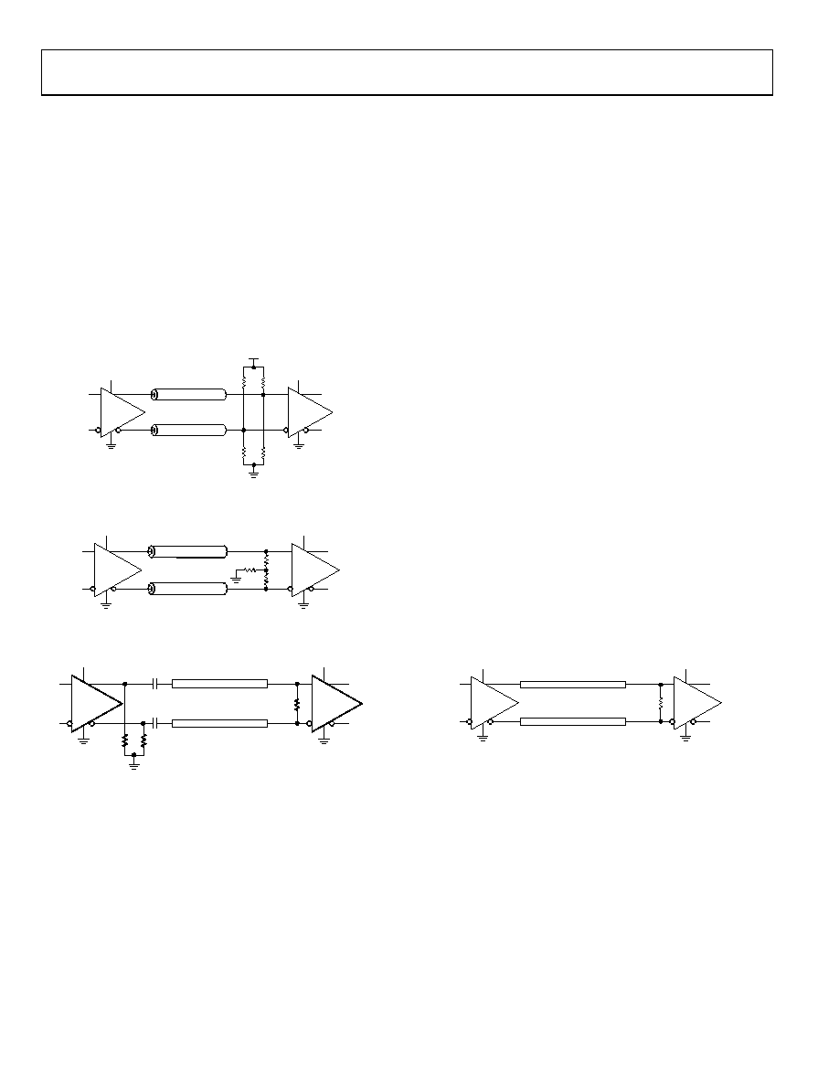
LVPECL CLOCK DISTRIBUTION
The LVPECL outputs of the AD9516 provide the lowest jitter
clock signals that are available from the AD9516. The LVPECL
outputs (because they are open emitter) require a dc termination
to bias the output transistors. The simplified equivalent circuit
in Figure 59 shows the LVPECL output stage.
In most applications, an LVPECL far-end Thevenin termination
(see Figure 71) or Y-termination (see Figure 72) is recommended.
In each case, the VS of the receiving buffer should match the
VS_LVPECL. If it does not, ac coupling is recommended (see
The resistor network is designed to match the transmission line
impedance (50 ) and the switching threshold (VS 1.3 V).
VS_LVPECL
LVPECL
50
SINGLE-ENDED
(NOT COUPLED)
VS
VS_DRV
LVPECL
127
83
06420-
145
Figure 71. DC-Coupled 3.3 V LVPECL, Far-End Thevenin Termination
VS_LVPECL
LVPECL
Z0 = 50
VS = 3.3V
LVPECL
50
Z0 = 50
06420-
147
Figure 72. DC-Coupled 3.3 V LVPECL, Y-Termination
VS_LVPECL
LVPECL
100 DIFFERENTIAL
(COUPLED)
TRANSMISSION LINE
VS
LVPECL
100
0.1nF
200
06420-
146
Figure 73. AC-Coupled LVPECL with Parallel Transmission Line
LVPECL Y-termination is an elegant termination scheme that
uses the fewest components and offers both odd- and even-mode
impedance matching. Even-mode impedance matching is an
important consideration for closely coupled transmission lines
at high frequencies. Its main drawback is that it offers limited
flexibility for varying the drive strength of the emitter-follower
LVPECL driver. This can be an important consideration when
driving long trace lengths but is usually not an issue. In the case
shown in Figure 72, where VS_LVPECL = 2.5 V, the 50
termination resistor that is connected to ground should be
changed to 19 .
Thevenin-equivalent termination uses a resistor network to provide
50 termination to a dc voltage that is below VOL of the LVPECL
driver. In this case, VS_LVPECL on the AD9516 should equal VS
of the receiving buffer. Although the resistor combination shown
in Figure 72 results in a dc bias point of VS_LVPECL 2 V, the
actual common-mode voltage is VS_LVPECL 1.3 V because
additional current flows from the AD9516 LVPECL driver through
the pull-down resistor.
The circuit is identical when VS_LVPECL = 2.5 V, except that
the pull-down resistor is 62.5 and the pull-up resistor is 250 .
LVDS CLOCK DISTRIBUTION
The AD9516 provides four clock outputs (OUT6 to OUT9) that
are selectable as either CMOS or LVDS level outputs. LVDS is a
differential output option that uses a current mode output stage.
The nominal current is 3.5 mA, which yields 350 mV output swing
across a 100 resistor. An output current of 7 mA is also available
in cases where a larger output swing is required. The LVDS
output meets or exceeds all ANSI/TIA/EIA-644 specifications.
A recommended termination circuit for the LVDS outputs is
shown in Figure 74.
VS
LVDS
100
DIFFERENTIAL (COUPLED)
VS
LVDS
100
06420-
047
Figure 74. LVDS Output Termination
See the AN-586 Application Note, LVDS Data Outputs for High-
Speed Analog-to-Digital Converters for more information on LVDS.
相关PDF资料 |
PDF描述 |
|---|---|
| MAX876AESA+T | IC VREF SERIES PREC 10V 8-SOIC |
| 35PX22MEFC5X11 | CAP ALUM 22UF 35V 20% RADIAL |
| GCC07DRYS-S734 | CONN EDGECARD 14POS DIP .100 SLD |
| MAX6177BASA+ | IC VREF SERIES PREC 3.3V 8-SOIC |
| AD9516-4/PCBZ | BOARD EVAL FOR AD9516-4 1.8GHZ |
相关代理商/技术参数 |
参数描述 |
|---|---|
| AD9516-1XCPZ | 制造商:Analog Devices 功能描述:14-CHANNEL CLOCK GENERATOR WITH INTEGRATED 2.8 GHZ VCO - Bulk |
| AD9516-2 | 制造商:AD 制造商全称:Analog Devices 功能描述:14-Output Clock Generator with Integrated 2.2 GHz VCO |
| AD9516-2/PCBZ | 功能描述:BOARD EVAL FOR AD9516-2 2.2GHZ RoHS:是 类别:编程器,开发系统 >> 评估演示板和套件 系列:- 标准包装:1 系列:- 主要目的:电信,线路接口单元(LIU) 嵌入式:- 已用 IC / 零件:IDT82V2081 主要属性:T1/J1/E1 LIU 次要属性:- 已供物品:板,电源,线缆,CD 其它名称:82EBV2081 |
| AD9516-2BCPZ | 功能描述:IC CLOCK PLL/VCO 2.2GHZ 64LFCSP RoHS:是 类别:集成电路 (IC) >> 时钟/计时 - 时钟发生器,PLL,频率合成器 系列:- 标准包装:2,000 系列:- 类型:PLL 时钟发生器 PLL:带旁路 输入:LVCMOS,LVPECL 输出:LVCMOS 电路数:1 比率 - 输入:输出:2:11 差分 - 输入:输出:是/无 频率 - 最大:240MHz 除法器/乘法器:是/无 电源电压:3.135 V ~ 3.465 V 工作温度:0°C ~ 70°C 安装类型:表面贴装 封装/外壳:32-LQFP 供应商设备封装:32-TQFP(7x7) 包装:带卷 (TR) |
| AD9516-2BCPZ-REEL7 | 功能描述:IC CLOCK PLL/VCO 2.2GHZ 64LFCSP RoHS:是 类别:集成电路 (IC) >> 时钟/计时 - 时钟发生器,PLL,频率合成器 系列:- 标准包装:2,000 系列:- 类型:PLL 时钟发生器 PLL:带旁路 输入:LVCMOS,LVPECL 输出:LVCMOS 电路数:1 比率 - 输入:输出:2:11 差分 - 输入:输出:是/无 频率 - 最大:240MHz 除法器/乘法器:是/无 电源电压:3.135 V ~ 3.465 V 工作温度:0°C ~ 70°C 安装类型:表面贴装 封装/外壳:32-LQFP 供应商设备封装:32-TQFP(7x7) 包装:带卷 (TR) |
发布紧急采购,3分钟左右您将得到回复。