- 您现在的位置:买卖IC网 > PDF目录16847 > AD9516-1/PCBZ (Analog Devices Inc)BOARD EVALUATION FOR AD9516-1 PDF资料下载
参数资料
| 型号: | AD9516-1/PCBZ |
| 厂商: | Analog Devices Inc |
| 文件页数: | 22/80页 |
| 文件大小: | 0K |
| 描述: | BOARD EVALUATION FOR AD9516-1 |
| 产品培训模块: | Active Filter Design Tools |
| 设计资源: | AD9516 Eval Brd Schematic AD9516 Gerber Files AD9516-1 BOM |
| 标准包装: | 1 |
| 主要目的: | 计时,时钟发生器 |
| 嵌入式: | 否 |
| 已用 IC / 零件: | AD9516-1 |
| 主要属性: | 2 输入,14 输出,2.5GHz VCO |
| 次要属性: | CMOS、LVDS、LVPECL 输出逻辑,ADIsimCLK&trade 图形用户界面 |
| 已供物品: | 板,线缆,电源 |
| 产品目录页面: | 776 (CN2011-ZH PDF) |
| 相关产品: | AD9516-1BCPZ-REEL7-ND - IC CLOCK GEN 2.5GHZ VCO 64-LFCSP AD9516-1BCPZ-ND - IC CLOCK GEN 2.5GHZ VCO 64-LFCSP |
第1页第2页第3页第4页第5页第6页第7页第8页第9页第10页第11页第12页第13页第14页第15页第16页第17页第18页第19页第20页第21页当前第22页第23页第24页第25页第26页第27页第28页第29页第30页第31页第32页第33页第34页第35页第36页第37页第38页第39页第40页第41页第42页第43页第44页第45页第46页第47页第48页第49页第50页第51页第52页第53页第54页第55页第56页第57页第58页第59页第60页第61页第62页第63页第64页第65页第66页第67页第68页第69页第70页第71页第72页第73页第74页第75页第76页第77页第78页第79页第80页
Data Sheet
AD9516-1
Rev. C | Page 29 of 80
PROGRAMMABLE
N DELAY
REFIN (REF1)
REFIN (REF2)
CLK
REF1
REF2
AD9516-1
STATUS
R
DIVIDER
VCO STATUS
PROGRAMMABLE
R DELAY
REFERENCE
SWITCHOVER
REF_SEL
CPRSET VCP
VS
GND
RSET
DISTRIBUTION
REFERENCE
REFMON
CP
STATUS
LD
P, P + 1
PRESCALER
A/B
COUNTERS
N DIVIDER
BYPASS
LF
LOW DROPOUT
REGULATOR (LDO)
VCO
PHASE
FREQUENCY
DETECTOR
LOCK
DETECT
CHARGE
PUMP
PL
L
RE
F
E
R
E
NCE
HOLD
OUT0
OUT1
OUT0
OUT1
LVPECL
DIVIDE BY
1 TO 32
OUT2
OUT3
OUT2
OUT3
LVPECL
DIVIDE BY
1 TO 32
OUT4
OUT5
OUT4
OUT5
LVPECL
DIVIDE BY
1 TO 32
DIVIDE BY
1 TO 32
LVDS/CMOS
OUT6 (OUT6A)
OUT6 (OUT6B)
t
OUT7 (OUT7A)
OUT7 (OUT7B)
t
DIVIDE BY
1 TO 32
DIVIDE BY
1 TO 32
LVDS/CMOS
OUT8 (OUT8A)
OUT8 (OUT8B)
t
OUT9 (OUT9A)
OUT9 (OUT9B)
t
DIVIDE BY
1 TO 32
0
1
DIVIDE BY
2, 3, 4, 5, OR 6
PD
SYNC
RESET
SCLK
SDIO
SDO
CS
DIGITAL
LOGIC
SERIAL
CONTROL
PORT
0
64
20-
0
30
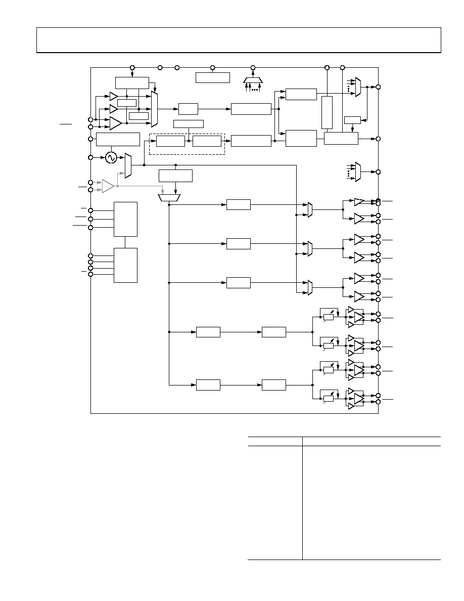
Figure 44. Internal VCO and Clock Distribution
Internal VCO and Clock Distribution
When using the internal VCO and PLL, the VCO divider must
be employed to ensure that the frequency presented to the
channel dividers does not exceed their specified maximum
frequency of 1600 MHz (see Table 3). The internal PLL uses an
external loop filter to set the loop bandwidth. The external loop
filter is also crucial to the loop stability.
When using the internal VCO, it is necessary to calibrate the
VCO (Register 0x018[0]) to ensure optimal performance.
For internal VCO and clock distribution applications, use the
register settings that are shown in Table 24.
Table 24. Settings When Using Internal VCO
Register
Function
0x010[1:0] = 00b
PLL normal operation (PLL on).
0x010 to 0x01E
PLL settings. Select and enable a reference
input; set R, N (P, A, B), PFD polarity, and ICP,
according to the intended loop configuration.
0x018[0] = 0b,
0x232[0] = 1b
Reset VCO calibration. This is not required
the first time after power-up, but it must
be performed subsequently.
0x1E0[2:0]
Set VCO divider to divide-by-2, divide-by-3,
divide-by-4, divide-by-5, and divide-by-6.
0x1E1[0] = 0b
Use the VCO divider as source for the
distribution section.
0x1E1[1] = 1b
Select VCO as the source.
0x018[0] = 1b,
0x232[0] = 1b
Initiate VCO calibration.
相关PDF资料 |
PDF描述 |
|---|---|
| MAX876AESA+T | IC VREF SERIES PREC 10V 8-SOIC |
| 35PX22MEFC5X11 | CAP ALUM 22UF 35V 20% RADIAL |
| GCC07DRYS-S734 | CONN EDGECARD 14POS DIP .100 SLD |
| MAX6177BASA+ | IC VREF SERIES PREC 3.3V 8-SOIC |
| AD9516-4/PCBZ | BOARD EVAL FOR AD9516-4 1.8GHZ |
相关代理商/技术参数 |
参数描述 |
|---|---|
| AD9516-1XCPZ | 制造商:Analog Devices 功能描述:14-CHANNEL CLOCK GENERATOR WITH INTEGRATED 2.8 GHZ VCO - Bulk |
| AD9516-2 | 制造商:AD 制造商全称:Analog Devices 功能描述:14-Output Clock Generator with Integrated 2.2 GHz VCO |
| AD9516-2/PCBZ | 功能描述:BOARD EVAL FOR AD9516-2 2.2GHZ RoHS:是 类别:编程器,开发系统 >> 评估演示板和套件 系列:- 标准包装:1 系列:- 主要目的:电信,线路接口单元(LIU) 嵌入式:- 已用 IC / 零件:IDT82V2081 主要属性:T1/J1/E1 LIU 次要属性:- 已供物品:板,电源,线缆,CD 其它名称:82EBV2081 |
| AD9516-2BCPZ | 功能描述:IC CLOCK PLL/VCO 2.2GHZ 64LFCSP RoHS:是 类别:集成电路 (IC) >> 时钟/计时 - 时钟发生器,PLL,频率合成器 系列:- 标准包装:2,000 系列:- 类型:PLL 时钟发生器 PLL:带旁路 输入:LVCMOS,LVPECL 输出:LVCMOS 电路数:1 比率 - 输入:输出:2:11 差分 - 输入:输出:是/无 频率 - 最大:240MHz 除法器/乘法器:是/无 电源电压:3.135 V ~ 3.465 V 工作温度:0°C ~ 70°C 安装类型:表面贴装 封装/外壳:32-LQFP 供应商设备封装:32-TQFP(7x7) 包装:带卷 (TR) |
| AD9516-2BCPZ-REEL7 | 功能描述:IC CLOCK PLL/VCO 2.2GHZ 64LFCSP RoHS:是 类别:集成电路 (IC) >> 时钟/计时 - 时钟发生器,PLL,频率合成器 系列:- 标准包装:2,000 系列:- 类型:PLL 时钟发生器 PLL:带旁路 输入:LVCMOS,LVPECL 输出:LVCMOS 电路数:1 比率 - 输入:输出:2:11 差分 - 输入:输出:是/无 频率 - 最大:240MHz 除法器/乘法器:是/无 电源电压:3.135 V ~ 3.465 V 工作温度:0°C ~ 70°C 安装类型:表面贴装 封装/外壳:32-LQFP 供应商设备封装:32-TQFP(7x7) 包装:带卷 (TR) |
发布紧急采购,3分钟左右您将得到回复。