- 您现在的位置:买卖IC网 > PDF目录16847 > AD9516-1/PCBZ (Analog Devices Inc)BOARD EVALUATION FOR AD9516-1 PDF资料下载
参数资料
| 型号: | AD9516-1/PCBZ |
| 厂商: | Analog Devices Inc |
| 文件页数: | 27/80页 |
| 文件大小: | 0K |
| 描述: | BOARD EVALUATION FOR AD9516-1 |
| 产品培训模块: | Active Filter Design Tools |
| 设计资源: | AD9516 Eval Brd Schematic AD9516 Gerber Files AD9516-1 BOM |
| 标准包装: | 1 |
| 主要目的: | 计时,时钟发生器 |
| 嵌入式: | 否 |
| 已用 IC / 零件: | AD9516-1 |
| 主要属性: | 2 输入,14 输出,2.5GHz VCO |
| 次要属性: | CMOS、LVDS、LVPECL 输出逻辑,ADIsimCLK&trade 图形用户界面 |
| 已供物品: | 板,线缆,电源 |
| 产品目录页面: | 776 (CN2011-ZH PDF) |
| 相关产品: | AD9516-1BCPZ-REEL7-ND - IC CLOCK GEN 2.5GHZ VCO 64-LFCSP AD9516-1BCPZ-ND - IC CLOCK GEN 2.5GHZ VCO 64-LFCSP |
第1页第2页第3页第4页第5页第6页第7页第8页第9页第10页第11页第12页第13页第14页第15页第16页第17页第18页第19页第20页第21页第22页第23页第24页第25页第26页当前第27页第28页第29页第30页第31页第32页第33页第34页第35页第36页第37页第38页第39页第40页第41页第42页第43页第44页第45页第46页第47页第48页第49页第50页第51页第52页第53页第54页第55页第56页第57页第58页第59页第60页第61页第62页第63页第64页第65页第66页第67页第68页第69页第70页第71页第72页第73页第74页第75页第76页第77页第78页第79页第80页
Data Sheet
AD9516-1
Rev. C | Page 33 of 80
Charge Pump (CP)
The charge pump is controlled by the PFD. The PFD monitors
the phase and frequency relationship between its two inputs,
and tells the CP to pump up or pump down to charge or discharge
the integrating node (part of the loop filter). The integrated and
filtered CP current is transformed into a voltage that drives the
tuning node of the internal VCO through the LF pin (or the tuning
pin of an external VCO) to move the VCO frequency up or down.
The CP can be set (Register 0x010[6:4]) for high impedance
(allows holdover operation), for normal operation (attempts to
lock the PLL loop), for pump up, or for pump down (test modes).
The CP current is programmable in eight steps from (nominally)
600 A to 4.8 mA. The exact value of the CP current LSB is set
by the CPRSET resistor, which is nominally 5.1 k. If the value
of the resistor connected to the CP_RSET pin is doubled, the
resulting charge pump current range becomes 300 A to 2.4 mA.
On-Chip VCO
The AD9516 includes an on-chip VCO covering the frequency
range shown in Table 2. The calibration procedure ensures that
the VCO operating voltage is centered for the desired VCO
frequency. The VCO must be calibrated when the VCO loop is first
set up, as well as any time the nominal VCO frequency changes.
However, once the VCO is calibrated, the VCO has sufficient
operating range to stay locked over temperature and voltage
extremes without needing additional calibration. See the VCO
Calibration section for more information.
The on-chip VCO is powered by an on-chip, low dropout
(LDO), linear voltage regulator. The LDO provides some
isolation of the VCO from variations in the power supply
voltage level. The BYPASS pin should be connected to ground
by a 220 nF capacitor to ensure stability. This LDO employs the
same technology used in the anyCAP line of regulators from
Analog Devices, Inc., making it insensitive to the type of
capacitor used. Driving an external load from the BYPASS pin
is not supported.
Note that the reference input signal must be present and the
VCO divider must not be static during VCO calibration.
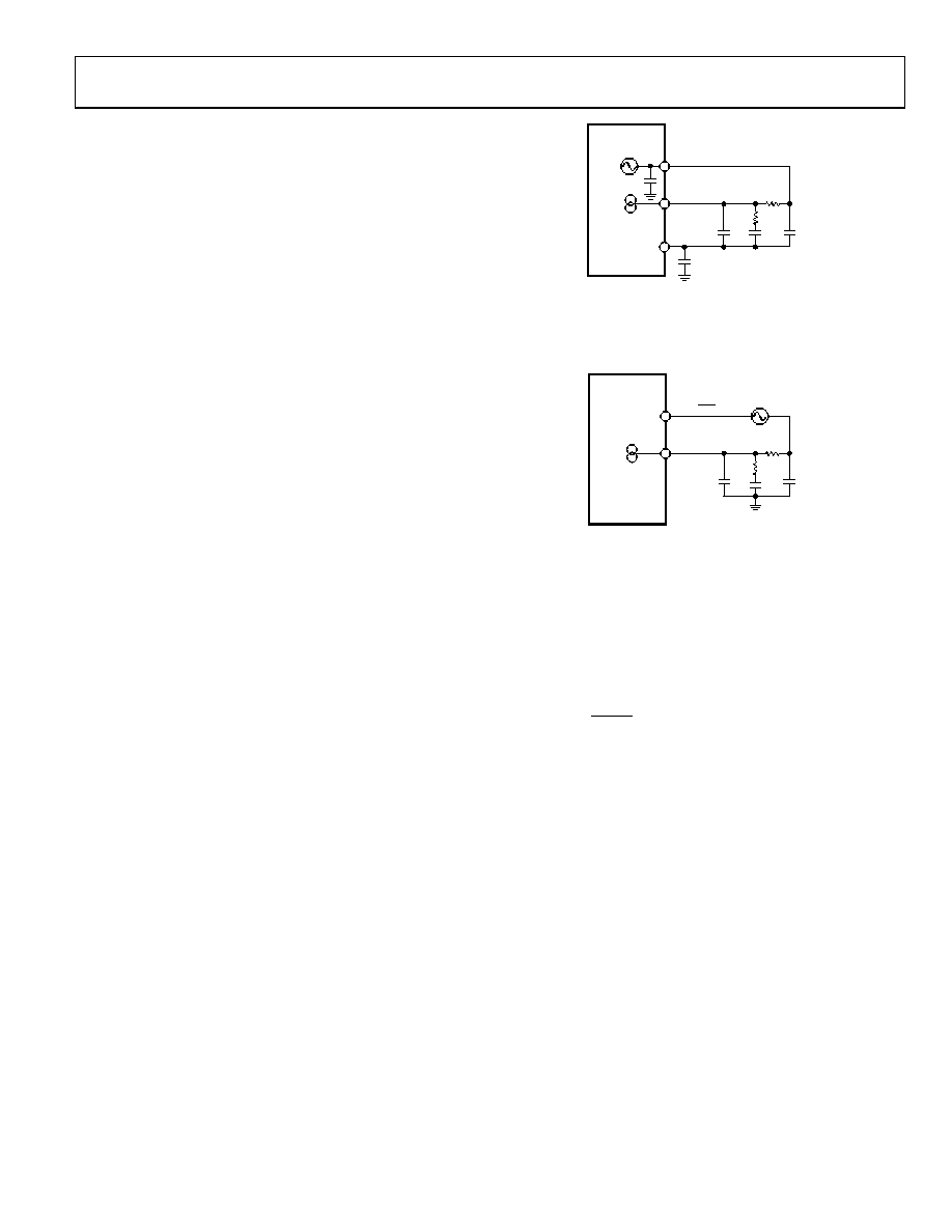
PLL External Loop Filter
When using the internal VCO, the external loop filter should
be referenced to the BYPASS pin for optimal noise and spurious
performance. An example of an external loop filter for a PLL
that uses the internal VCO is shown in Figure 47. The third-
order design shown in Figure 47 usually offers best performance.
A loop filter must be calculated for each desired PLL configuration.
The values of the components depend upon the VCO frequency,
the KVCO, the PFD frequency, the CP current, the desired loop
bandwidth, and the desired phase margin. The loop filter affects
the phase noise, the loop settling time, and loop stability. A basic
knowledge of PLL theory is helpful for understanding loop filter
design. ADIsimCLK can help with calculation of a loop filter
according to application requirements.
LF
VCO
CHARGE
PUMP
CP
BYPASS
C1
C2
C3
R1
31pF
R2
CBP = 220nF
AD9516-1
06420-
065
Figure 47. Example of External Loop Filter for a PLL Using the Internal VCO
When using an external VCO, the external loop filter should be
referenced to ground. See Figure 48 for an example of an
external loop filter for a PLL using an external VCO.
CLK/CLK
EXTERNAL
VCO/VCXO
CHARGE
PUMP
CP
C1
C2
C3
R1
R2
AD9516-1
06420-
265
Figure 48. Example of External Loop Filter for a PLL Using an External VCO
PLL Reference Inputs
The AD9516 features a flexible PLL reference input circuit that
allows either a fully differential input or two separate single-
ended inputs. The input frequency range for the reference
inputs is specified in Table 2. Both the differential and the
single-ended inputs are self-biased, allowing for easy ac
coupling of input signals.
The differential input and the single-ended inputs share the two
pins, REFIN/REFIN (REF1 and REF2, respectively). The desired
reference input type is selected and controlled by Register 0x01C
When the differential reference input is selected, the self-bias
level of the two sides is offset slightly (~100 mV, see Table 2) to
prevent chattering of the input buffer when the reference is slow
or missing. This increases the voltage swing that is required of the
driver and overcomes the offset. The differential reference input
can be driven by either ac-coupled LVDS or ac-coupled LVPECL
signals.
The single-ended inputs can be driven by either a dc-coupled
CMOS level signal or an ac-coupled sine wave or square wave.
Each single-ended input can be independently powered down
when not needed to increase isolation and reduce power. Either
a differential or a single-ended reference must be specifically
enabled. All PLL reference inputs are off by default.
The differential reference input is powered down whenever the
PLL is powered down, or when the differential reference input
is not selected. The single-ended buffers power down when the
PLL is powered down, and when their individual power down
registers are set. When the differential mode is selected, the
single-ended inputs are powered down.
相关PDF资料 |
PDF描述 |
|---|---|
| MAX876AESA+T | IC VREF SERIES PREC 10V 8-SOIC |
| 35PX22MEFC5X11 | CAP ALUM 22UF 35V 20% RADIAL |
| GCC07DRYS-S734 | CONN EDGECARD 14POS DIP .100 SLD |
| MAX6177BASA+ | IC VREF SERIES PREC 3.3V 8-SOIC |
| AD9516-4/PCBZ | BOARD EVAL FOR AD9516-4 1.8GHZ |
相关代理商/技术参数 |
参数描述 |
|---|---|
| AD9516-1XCPZ | 制造商:Analog Devices 功能描述:14-CHANNEL CLOCK GENERATOR WITH INTEGRATED 2.8 GHZ VCO - Bulk |
| AD9516-2 | 制造商:AD 制造商全称:Analog Devices 功能描述:14-Output Clock Generator with Integrated 2.2 GHz VCO |
| AD9516-2/PCBZ | 功能描述:BOARD EVAL FOR AD9516-2 2.2GHZ RoHS:是 类别:编程器,开发系统 >> 评估演示板和套件 系列:- 标准包装:1 系列:- 主要目的:电信,线路接口单元(LIU) 嵌入式:- 已用 IC / 零件:IDT82V2081 主要属性:T1/J1/E1 LIU 次要属性:- 已供物品:板,电源,线缆,CD 其它名称:82EBV2081 |
| AD9516-2BCPZ | 功能描述:IC CLOCK PLL/VCO 2.2GHZ 64LFCSP RoHS:是 类别:集成电路 (IC) >> 时钟/计时 - 时钟发生器,PLL,频率合成器 系列:- 标准包装:2,000 系列:- 类型:PLL 时钟发生器 PLL:带旁路 输入:LVCMOS,LVPECL 输出:LVCMOS 电路数:1 比率 - 输入:输出:2:11 差分 - 输入:输出:是/无 频率 - 最大:240MHz 除法器/乘法器:是/无 电源电压:3.135 V ~ 3.465 V 工作温度:0°C ~ 70°C 安装类型:表面贴装 封装/外壳:32-LQFP 供应商设备封装:32-TQFP(7x7) 包装:带卷 (TR) |
| AD9516-2BCPZ-REEL7 | 功能描述:IC CLOCK PLL/VCO 2.2GHZ 64LFCSP RoHS:是 类别:集成电路 (IC) >> 时钟/计时 - 时钟发生器,PLL,频率合成器 系列:- 标准包装:2,000 系列:- 类型:PLL 时钟发生器 PLL:带旁路 输入:LVCMOS,LVPECL 输出:LVCMOS 电路数:1 比率 - 输入:输出:2:11 差分 - 输入:输出:是/无 频率 - 最大:240MHz 除法器/乘法器:是/无 电源电压:3.135 V ~ 3.465 V 工作温度:0°C ~ 70°C 安装类型:表面贴装 封装/外壳:32-LQFP 供应商设备封装:32-TQFP(7x7) 包装:带卷 (TR) |
发布紧急采购,3分钟左右您将得到回复。