- 您现在的位置:买卖IC网 > PDF目录16847 > AD9516-1/PCBZ (Analog Devices Inc)BOARD EVALUATION FOR AD9516-1 PDF资料下载
参数资料
| 型号: | AD9516-1/PCBZ |
| 厂商: | Analog Devices Inc |
| 文件页数: | 72/80页 |
| 文件大小: | 0K |
| 描述: | BOARD EVALUATION FOR AD9516-1 |
| 产品培训模块: | Active Filter Design Tools |
| 设计资源: | AD9516 Eval Brd Schematic AD9516 Gerber Files AD9516-1 BOM |
| 标准包装: | 1 |
| 主要目的: | 计时,时钟发生器 |
| 嵌入式: | 否 |
| 已用 IC / 零件: | AD9516-1 |
| 主要属性: | 2 输入,14 输出,2.5GHz VCO |
| 次要属性: | CMOS、LVDS、LVPECL 输出逻辑,ADIsimCLK&trade 图形用户界面 |
| 已供物品: | 板,线缆,电源 |
| 产品目录页面: | 776 (CN2011-ZH PDF) |
| 相关产品: | AD9516-1BCPZ-REEL7-ND - IC CLOCK GEN 2.5GHZ VCO 64-LFCSP AD9516-1BCPZ-ND - IC CLOCK GEN 2.5GHZ VCO 64-LFCSP |
第1页第2页第3页第4页第5页第6页第7页第8页第9页第10页第11页第12页第13页第14页第15页第16页第17页第18页第19页第20页第21页第22页第23页第24页第25页第26页第27页第28页第29页第30页第31页第32页第33页第34页第35页第36页第37页第38页第39页第40页第41页第42页第43页第44页第45页第46页第47页第48页第49页第50页第51页第52页第53页第54页第55页第56页第57页第58页第59页第60页第61页第62页第63页第64页第65页第66页第67页第68页第69页第70页第71页当前第72页第73页第74页第75页第76页第77页第78页第79页第80页
AD9516-1
Data Sheet
Rev. C | Page 74 of 80
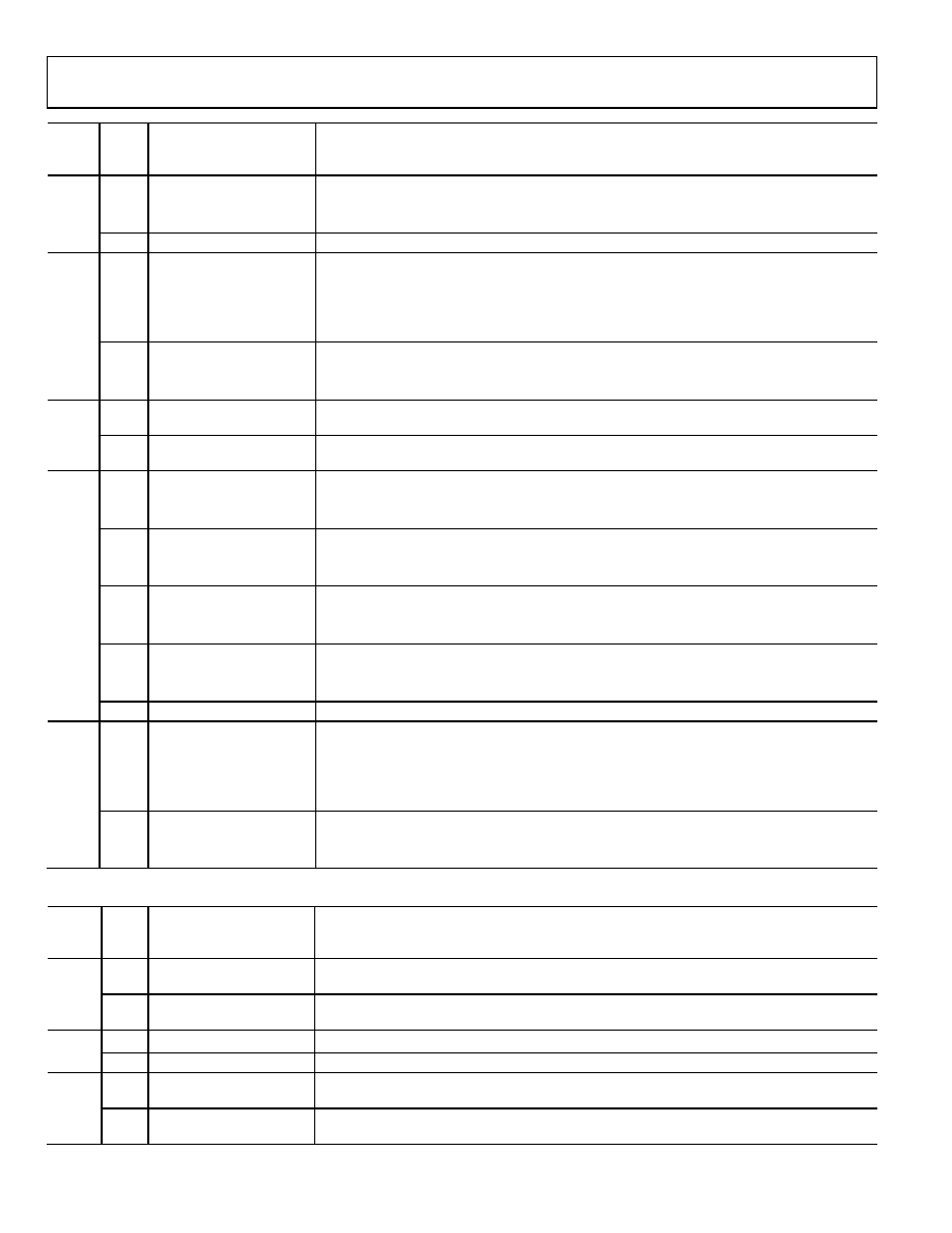
Reg.
Addr.
(Hex)
Bits
Name
Description
0x194
4
Divider 1 start high
Selects clock output to start high or start low.
0: starts low (default).
1: starts high.
[3:0]
Divider 1 phase offset
Phase offset (default = 0x0).
0x195
1
Divider 1 direct to output
Connects OUT2 and OUT3 to Divider 1 or directly to VCO or CLK.
0: OUT2 and OUT3 are connected to Divider 1 (default).
1: If Register 0x1E1[1:0] = 10b, the VCO is routed directly to OUT2 and OUT3.
If Register 0x1E1[1:0] = 00b, the CLK is routed directly to OUT2 and OUT3.
If Register 0x1E1[1:0] = 01b, there is no effect.
0
Divider 1 DCCOFF
Duty-cycle correction function.
0: enables duty-cycle correction (default).
1: disables duty-cycle correction.
0x196
[7:4]
Divider 2 low cycles
Number of clock cycles (minus 1) of the divider input during which divider output stays low.
A value of 0x0 means that the divider is low for one input clock cycle (default = 0x0).
[3:0]
Divider 2 high cycles
Number of clock cycles (minus 1) of the divider input during which divider output stays high.
A value of 0x0 means that the divider is high for one input clock cycle (default = 0x0).
0x197
7
Divider 2 bypass
Bypasses and powers down the divider; routes input to divider output.
0: uses divider.
1: bypasses divider (default).
6
Divider 2 nosync
Nosync.
0: obeys chip-level SYNC signal (default).
1: ignores chip-level SYNC signal.
5
Divider 2 force high
Forces divider output to high. This requires that nosync (Bit 6) also be set.
0: divider output forced to low (default).
1: divider output forced to high.
4
Divider 2 start high
Selects clock output to start high or start low.
0: starts low (default).
1: starts high.
[3:0]
Divider 2 phase offset
Phase offset (default = 0x0).
0x198
1
Divider 2 direct to output
Connects OUT4 and OUT5 to Divider 2 or directly to VCO or CLK.
0: OUT4 and OUT5 are connected to Divider 2 (default).
1: If Register 0x1E1[1:0] = 10b, the VCO is routed directly to OUT4 and OUT5.
If Register 0x1E1[1:0] = 00b, the CLK is routed directly to OUT4 and OUT5.
If Register 0x1E1[1:0] = 01b, there is no effect.
0
Divider 2 DCCOFF
Duty-cycle correction function.
0: enables duty-cycle correction (default).
1: disables duty-cycle correction.
Table 59. LVDS/CMOS Channel Dividers
Reg.
Addr.
(Hex)
Bits
Name
Description
0x199
[7:4]
Low Cycles Divider 3.1
Number of clock cycles (minus 1) of 3.1 divider input during which 3.1 output stays low.
A value of 0x0 means that the divider is low for one input clock cycle (default = 0x0).
[3:0]
High Cycles Divider 3.1
Number of clock cycles (minus 1) of 3.1 divider input during which 3.1 output stays high. A value of
0x0 means that the divider is high for one input clock cycle (default = 0x0).
0x19A
[7:4]
Phase Offset Divider 3.2
Refer to LVDS/CMOS channel divider function description (default = 0x0).
[3:0]
Phase Offset Divider 3.1
Refer to LVDS/CMOS channel divider function description (default = 0x0).
0x19B
[7:4]
Low Cycles Divider 3.2
Number of clock cycles (minus 1) of 3.2 divider input during which 3.2 output stays low.
A value of 0x0 means that the divider is low for one input clock cycle (default = 0x0).
[3:0]
High Cycles Divider 3.2
Number of clock cycles (minus 1)of 3.2 divider input during which 3.2 output stays high. A value
of 0x0 means that the divider is high for one input clock cycle (default = 0x0).
相关PDF资料 |
PDF描述 |
|---|---|
| MAX876AESA+T | IC VREF SERIES PREC 10V 8-SOIC |
| 35PX22MEFC5X11 | CAP ALUM 22UF 35V 20% RADIAL |
| GCC07DRYS-S734 | CONN EDGECARD 14POS DIP .100 SLD |
| MAX6177BASA+ | IC VREF SERIES PREC 3.3V 8-SOIC |
| AD9516-4/PCBZ | BOARD EVAL FOR AD9516-4 1.8GHZ |
相关代理商/技术参数 |
参数描述 |
|---|---|
| AD9516-1XCPZ | 制造商:Analog Devices 功能描述:14-CHANNEL CLOCK GENERATOR WITH INTEGRATED 2.8 GHZ VCO - Bulk |
| AD9516-2 | 制造商:AD 制造商全称:Analog Devices 功能描述:14-Output Clock Generator with Integrated 2.2 GHz VCO |
| AD9516-2/PCBZ | 功能描述:BOARD EVAL FOR AD9516-2 2.2GHZ RoHS:是 类别:编程器,开发系统 >> 评估演示板和套件 系列:- 标准包装:1 系列:- 主要目的:电信,线路接口单元(LIU) 嵌入式:- 已用 IC / 零件:IDT82V2081 主要属性:T1/J1/E1 LIU 次要属性:- 已供物品:板,电源,线缆,CD 其它名称:82EBV2081 |
| AD9516-2BCPZ | 功能描述:IC CLOCK PLL/VCO 2.2GHZ 64LFCSP RoHS:是 类别:集成电路 (IC) >> 时钟/计时 - 时钟发生器,PLL,频率合成器 系列:- 标准包装:2,000 系列:- 类型:PLL 时钟发生器 PLL:带旁路 输入:LVCMOS,LVPECL 输出:LVCMOS 电路数:1 比率 - 输入:输出:2:11 差分 - 输入:输出:是/无 频率 - 最大:240MHz 除法器/乘法器:是/无 电源电压:3.135 V ~ 3.465 V 工作温度:0°C ~ 70°C 安装类型:表面贴装 封装/外壳:32-LQFP 供应商设备封装:32-TQFP(7x7) 包装:带卷 (TR) |
| AD9516-2BCPZ-REEL7 | 功能描述:IC CLOCK PLL/VCO 2.2GHZ 64LFCSP RoHS:是 类别:集成电路 (IC) >> 时钟/计时 - 时钟发生器,PLL,频率合成器 系列:- 标准包装:2,000 系列:- 类型:PLL 时钟发生器 PLL:带旁路 输入:LVCMOS,LVPECL 输出:LVCMOS 电路数:1 比率 - 输入:输出:2:11 差分 - 输入:输出:是/无 频率 - 最大:240MHz 除法器/乘法器:是/无 电源电压:3.135 V ~ 3.465 V 工作温度:0°C ~ 70°C 安装类型:表面贴装 封装/外壳:32-LQFP 供应商设备封装:32-TQFP(7x7) 包装:带卷 (TR) |
发布紧急采购,3分钟左右您将得到回复。