- 您现在的位置:买卖IC网 > PDF目录16847 > AD9516-1/PCBZ (Analog Devices Inc)BOARD EVALUATION FOR AD9516-1 PDF资料下载
参数资料
| 型号: | AD9516-1/PCBZ |
| 厂商: | Analog Devices Inc |
| 文件页数: | 43/80页 |
| 文件大小: | 0K |
| 描述: | BOARD EVALUATION FOR AD9516-1 |
| 产品培训模块: | Active Filter Design Tools |
| 设计资源: | AD9516 Eval Brd Schematic AD9516 Gerber Files AD9516-1 BOM |
| 标准包装: | 1 |
| 主要目的: | 计时,时钟发生器 |
| 嵌入式: | 否 |
| 已用 IC / 零件: | AD9516-1 |
| 主要属性: | 2 输入,14 输出,2.5GHz VCO |
| 次要属性: | CMOS、LVDS、LVPECL 输出逻辑,ADIsimCLK&trade 图形用户界面 |
| 已供物品: | 板,线缆,电源 |
| 产品目录页面: | 776 (CN2011-ZH PDF) |
| 相关产品: | AD9516-1BCPZ-REEL7-ND - IC CLOCK GEN 2.5GHZ VCO 64-LFCSP AD9516-1BCPZ-ND - IC CLOCK GEN 2.5GHZ VCO 64-LFCSP |
第1页第2页第3页第4页第5页第6页第7页第8页第9页第10页第11页第12页第13页第14页第15页第16页第17页第18页第19页第20页第21页第22页第23页第24页第25页第26页第27页第28页第29页第30页第31页第32页第33页第34页第35页第36页第37页第38页第39页第40页第41页第42页当前第43页第44页第45页第46页第47页第48页第49页第50页第51页第52页第53页第54页第55页第56页第57页第58页第59页第60页第61页第62页第63页第64页第65页第66页第67页第68页第69页第70页第71页第72页第73页第74页第75页第76页第77页第78页第79页第80页
AD9516-1
Data Sheet
Rev. C | Page 48 of 80
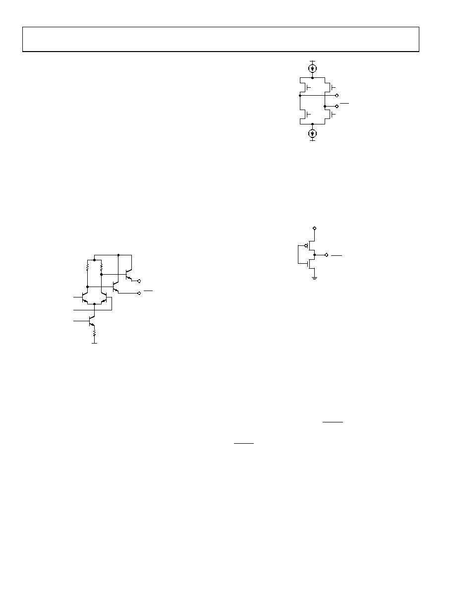
LVPECL Outputs—OUT0 to OUT5
The LVPECL differential voltage (VOD) is selectable from ~400 mV
to ~960 mV (see Register 0x0F0[3:2] to Register 0x0F5[3:2]).
The LVPECL outputs have dedicated pins for power supply
(VS_LVPECL), allowing a separate power supply to be used.
VS_LVPECL can be from 2.5 V to 3.3 V.
The LVPECL output polarity can be set as noninverting or
inverting, which allows for the adjustment of the relative
polarity of outputs within an application without requiring a
board layout change. Each LVPECL output can be powered
down or powered up, as needed. Because of the architecture of
the LVPECL output stages, there is the possibility of electrical
overstress and breakdown under certain power-down conditions.
For this reason, the LVPECL outputs have several power-down
modes. This includes a safe power-down mode that continues
to protect the output devices while powered down, although it
consumes somewhat more power than a total power-down. If
the LVPECL output pins are terminated, it is best to select the
safe power-down mode. If the pins are not connected (unused),
it is acceptable to use the total power-down mode.
GND
3.3V
OUT
06420-
033
Figure 59. LVPECL Output Simplified Equivalent Circuit
LVDS/CMOS Outputs—OUT6 to OUT9
OUT6 to OUT9 can be configured as either an LVDS
differential output or as a pair of CMOS single-ended outputs.
The LVDS outputs allow for selectable output current from
~1.75 mA to ~7 mA.
The LVDS output polarity can be set as noninverting or
inverting, which allows for the adjustment of the relative
polarity of outputs within an application without requiring a
board layout change. Each LVDS output can be powered down
if not needed to save power.
OUT6 to OUT9 can also be CMOS outputs. Each LVDS output
can be configured to be two CMOS outputs. This provides for
up to eight CMOS outputs: OUT6A, OUT6B, OUT7A, OUT7B,
OUT8A, OUT8B, OUT9A, and OUT9B. When an output is
configured as CMOS, CMOS Output A is automatically turned on.
CMOS Output B can be turned on or off independently. The
relative polarity of the CMOS outputs can also be selected for any
combination of inverting and noninverting (see Table 57 for
Register 0x140[7:5], Register 0x141[7:5], Register 0x142[7:5],
and Register 0x143[7:5]).
OUT
3.5mA
06420-
034
Figure 60. LVDS Output Simplified Equivalent Circuit with
3.5 mA Typical Current Source
Each LVDS/CMOS output can be powered down as needed to
save power. The CMOS output power-down is controlled by the
same bit that controls the LVDS power-down for that output.
This power-down control affects both CMOS Output A and
CMOS Output B. However, when CMOS Output A is powered up,
CMOS Output B can be powered on or off separately.
OUT1/
OUT1
VS
06420-
035
Figure 61. CMOS Equivalent Output Circuit
RESET MODES
The AD9516 has several ways to force the chip into a reset
condition that restores all registers to their default values and
makes these settings active.
Power-On Reset—Start-Up Conditions When VS Is
Applied
A power-on reset (POR) is issued when the VS power supply is
turned on. This initializes the chip to the power-on conditions
that are determined by the default register settings. These are
indicated in the Default Value (Hex) column of Table 52. At
power-on, the AD9516 also executes a SYNC operation, which
brings the outputs into phase alignment according to the default
settings.
Asynchronous Reset via the RESET Pin
An asynchronous hard reset is executed by momentarily pulling
RESET low. A reset restores the chip registers to the default settings.
Soft Reset via Register 0x000[2]
A soft reset is executed by writing Register 0x000[2] and
Register 0x000[5] = 1b. This bit is not self-clearing; it must be
cleared by writing Register 0x000[2] and Register 0x000[5] = 0b to
reset it and complete the soft reset operation. A soft reset restores
the default values to the internal registers. The soft reset bit does
not require an update registers command (Register 0x232) to be
issued.
相关PDF资料 |
PDF描述 |
|---|---|
| MAX876AESA+T | IC VREF SERIES PREC 10V 8-SOIC |
| 35PX22MEFC5X11 | CAP ALUM 22UF 35V 20% RADIAL |
| GCC07DRYS-S734 | CONN EDGECARD 14POS DIP .100 SLD |
| MAX6177BASA+ | IC VREF SERIES PREC 3.3V 8-SOIC |
| AD9516-4/PCBZ | BOARD EVAL FOR AD9516-4 1.8GHZ |
相关代理商/技术参数 |
参数描述 |
|---|---|
| AD9516-1XCPZ | 制造商:Analog Devices 功能描述:14-CHANNEL CLOCK GENERATOR WITH INTEGRATED 2.8 GHZ VCO - Bulk |
| AD9516-2 | 制造商:AD 制造商全称:Analog Devices 功能描述:14-Output Clock Generator with Integrated 2.2 GHz VCO |
| AD9516-2/PCBZ | 功能描述:BOARD EVAL FOR AD9516-2 2.2GHZ RoHS:是 类别:编程器,开发系统 >> 评估演示板和套件 系列:- 标准包装:1 系列:- 主要目的:电信,线路接口单元(LIU) 嵌入式:- 已用 IC / 零件:IDT82V2081 主要属性:T1/J1/E1 LIU 次要属性:- 已供物品:板,电源,线缆,CD 其它名称:82EBV2081 |
| AD9516-2BCPZ | 功能描述:IC CLOCK PLL/VCO 2.2GHZ 64LFCSP RoHS:是 类别:集成电路 (IC) >> 时钟/计时 - 时钟发生器,PLL,频率合成器 系列:- 标准包装:2,000 系列:- 类型:PLL 时钟发生器 PLL:带旁路 输入:LVCMOS,LVPECL 输出:LVCMOS 电路数:1 比率 - 输入:输出:2:11 差分 - 输入:输出:是/无 频率 - 最大:240MHz 除法器/乘法器:是/无 电源电压:3.135 V ~ 3.465 V 工作温度:0°C ~ 70°C 安装类型:表面贴装 封装/外壳:32-LQFP 供应商设备封装:32-TQFP(7x7) 包装:带卷 (TR) |
| AD9516-2BCPZ-REEL7 | 功能描述:IC CLOCK PLL/VCO 2.2GHZ 64LFCSP RoHS:是 类别:集成电路 (IC) >> 时钟/计时 - 时钟发生器,PLL,频率合成器 系列:- 标准包装:2,000 系列:- 类型:PLL 时钟发生器 PLL:带旁路 输入:LVCMOS,LVPECL 输出:LVCMOS 电路数:1 比率 - 输入:输出:2:11 差分 - 输入:输出:是/无 频率 - 最大:240MHz 除法器/乘法器:是/无 电源电压:3.135 V ~ 3.465 V 工作温度:0°C ~ 70°C 安装类型:表面贴装 封装/外壳:32-LQFP 供应商设备封装:32-TQFP(7x7) 包装:带卷 (TR) |
发布紧急采购,3分钟左右您将得到回复。