- 您现在的位置:买卖IC网 > PDF目录1987 > AD9550BCPZ-REEL7 (Analog Devices Inc)IC INTEGER-N TRANSLATOR 32-LFCSP PDF资料下载
参数资料
| 型号: | AD9550BCPZ-REEL7 |
| 厂商: | Analog Devices Inc |
| 文件页数: | 8/20页 |
| 文件大小: | 0K |
| 描述: | IC INTEGER-N TRANSLATOR 32-LFCSP |
| 标准包装: | 1,500 |
| 类型: | 时钟/频率转换器 |
| PLL: | 是 |
| 主要目的: | 以太网,GPON,SONET/SHD,T1/E1 |
| 输入: | CMOS |
| 输出: | CMOS,LVDS,LVPECL |
| 电路数: | 1 |
| 比率 - 输入:输出: | 1:2 |
| 差分 - 输入:输出: | 无/是 |
| 频率 - 最大: | 810MHz |
| 电源电压: | 3.135 V ~ 3.465 V |
| 工作温度: | -40°C ~ 85°C |
| 安装类型: | 表面贴装 |
| 封装/外壳: | 32-WFQFN 裸露焊盘,CSP |
| 供应商设备封装: | 32-LFCSP-WQ |
| 包装: | 带卷 (TR) |
AD9550
Rev. 0 | Page 16 of 20
Output Dividers
The output divider section consists of three dividers: P0, P1, and P2.
The P0 divider (or VCO frequency prescaler) accepts the VCO
frequency and reduces it by an integer factor of 5 to 11, thereby
reducing the frequency to a range between 305 MHz and 810 MHz.
The output of the P0 divider independently drives the P1 divider
and the P2 divider. The P1 divider establishes the frequency at
OUT1 and the P2 divider establishes the frequency at OUT2.
The P1 and P2 dividers are each programmable over a range of
1 to 1023, which results in a frequency at OUT1 or OUT2 that
is an integer submultiple of the frequency at the output of the
P0 divider.
Output Driver Mode Control
Three mode control pins (OM0, OM1, and OM2) establish the
logic family and pin function of the output drivers. The logic
families include LVDS, LVPECL, and CMOS (see Table 10).
Table 10. Logic Family Assignment via the OMx Pins
Pin OMx
Logic Family
OUT1
OUT2
000
LVPECL
001
LVPECL
LVDS
010
LVDS
LVPECL
011
LVPECL
CMOS
100
LVDS
101
LVDS
CMOS
110
CMOS
LVDS
111
CMOS
Because both output drivers support the LVDS and LVPECL
logic families, each driver has two pins to handle the differential
signals associated with these two logic families. The OUT1 driver
uses the OUT1 and OUT1 pins, and the OUT2 driver uses the
OUT2 and OUT2 pins. When the OMx pins select the CMOS
logic family, the signal at the OUT1 pin is a phase aligned replica
of the signal at the OUT1 pin and the signal at the OUT2 pin is a
phase aligned replica of the signal at the OUT2 pin.
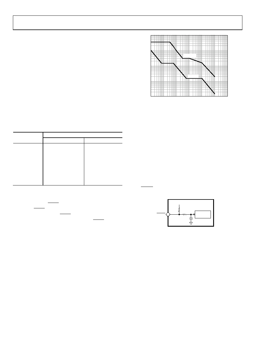
JITTER TOLERANCE
Jitter tolerance is the ability of the AD9550 to maintain lock in the
presence of sinusoidal jitter. The AD9550 meets the input jitter
tolerance mask per Telcordia GR-253-CORE (see Figure 25).
The acceptable jitter tolerance is the region above the mask.
0.1
1
10
100
1000
0.1
0.01
1
10
100
1M
10M
JITTER FREQUENCY (kHz)
IN
P
U
T
J
ITTE
R
A
M
P
LITU
D
E
(
U
Ip-
p)
AD9550
MASK
09057-
021
Figure 25. Jitter Tolerance
LOW DROPOUT (LDO) REGULATORS
The AD9550 is powered from a single 3.3 V supply and contains
on-chip LDO regulators for each function to eliminate the need
for external LDOs. To ensure optimal performance, each LDO
output should have a 0.47 μF capacitor connected between its
access pin and ground.
AUTOMATIC POWER-ON RESET
The AD9550 has an internal power-on reset circuit (see Figure 26).
At power-up, an 800 pF capacitor momentarily holds a Logic 0 at
the active low input of the reset circuitry. This ensures that the
device is held in a reset state (~250 s) until the capacitor charges
sufficiently via the 100 k pull-up resistor and 200 k series
resistor. Note that when using a low impedance source to drive
the RESET pin, be sure that the source is either tristate or Logic 0
at power-up; otherwise, the device may not calibrate properly.
15
RESET
200k
100k
800pF
VDD
RESET
CIRCUITRY
AD9550
09057-
022
Figure 26. Power-On Reset
Provided an input reference signal is present at the REF pin, the
device automatically performs a VCO calibration during power-up.
If the input reference signal is not present, VCO calibration fails
and the PLL does not lock. As soon as an input reference signal
is present, the user must reset the device to initiate the automatic
VCO calibration process.
Any change to the preset frequency selection pins requires the
user to reset the device. This is necessary to initiate the automatic
VCO calibration process.
相关PDF资料 |
PDF描述 |
|---|---|
| AD9551BCPZ | IC CLOCK GEN MULTISERV 40-LFCSP |
| AD9552BCPZ-REEL7 | IC PLL CLOCK GEN LP 32LFCSP |
| AD9553BCPZ-REEL7 | IC INTEGER-N CLCK GEN 32LFCSP |
| AD9557BCPZ-REEL7 | IC CLK XLATR PLL 1250MHZ 40LFCSP |
| AD9558BCPZ-REEL7 | IC CLK XLATR PLL 1250MHZ 64LFCSP |
相关代理商/技术参数 |
参数描述 |
|---|---|
| AD9551 | 制造商:AD 制造商全称:Analog Devices 功能描述:Multiservice Clock Generator |
| AD9551/PCBZ | 功能描述:BOARD EVAL FOR AD9951 RoHS:是 类别:编程器,开发系统 >> 评估演示板和套件 系列:- 标准包装:1 系列:PSoC® 主要目的:电源管理,热管理 嵌入式:- 已用 IC / 零件:- 主要属性:- 次要属性:- 已供物品:板,CD,电源 |
| AD9551BCPZ | 功能描述:IC CLOCK GEN MULTISERV 40-LFCSP RoHS:是 类别:集成电路 (IC) >> 时钟/计时 - 时钟发生器,PLL,频率合成器 系列:- 标准包装:2,000 系列:- 类型:PLL 时钟发生器 PLL:带旁路 输入:LVCMOS,LVPECL 输出:LVCMOS 电路数:1 比率 - 输入:输出:2:11 差分 - 输入:输出:是/无 频率 - 最大:240MHz 除法器/乘法器:是/无 电源电压:3.135 V ~ 3.465 V 工作温度:0°C ~ 70°C 安装类型:表面贴装 封装/外壳:32-LQFP 供应商设备封装:32-TQFP(7x7) 包装:带卷 (TR) |
| AD9551BCPZ-REEL7 | 功能描述:IC CLOCK GEN TRANSLATOR 40LFCSP RoHS:是 类别:集成电路 (IC) >> 时钟/计时 - 时钟发生器,PLL,频率合成器 系列:- 标准包装:2,000 系列:- 类型:PLL 时钟发生器 PLL:带旁路 输入:LVCMOS,LVPECL 输出:LVCMOS 电路数:1 比率 - 输入:输出:2:11 差分 - 输入:输出:是/无 频率 - 最大:240MHz 除法器/乘法器:是/无 电源电压:3.135 V ~ 3.465 V 工作温度:0°C ~ 70°C 安装类型:表面贴装 封装/外壳:32-LQFP 供应商设备封装:32-TQFP(7x7) 包装:带卷 (TR) |
| AD9552 | 制造商:AD 制造商全称:Analog Devices 功能描述:Oscillator Frequency Upconverter |
发布紧急采购,3分钟左右您将得到回复。