参数资料
| 型号: | AD9551BCPZ |
| 厂商: | Analog Devices Inc |
| 文件页数: | 1/40页 |
| 文件大小: | 0K |
| 描述: | IC CLOCK GEN MULTISERV 40-LFCSP |
| 标准包装: | 1 |
| 类型: | 时钟发生器 |
| PLL: | 是 |
| 输入: | 晶体 |
| 输出: | CMOS,LVDS,LVPECL |
| 电路数: | 1 |
| 比率 - 输入:输出: | 2:2 |
| 差分 - 输入:输出: | 是/是 |
| 频率 - 最大: | 900MHz |
| 除法器/乘法器: | 无/无 |
| 电源电压: | 3.3V |
| 工作温度: | -40°C ~ 85°C |
| 安装类型: | 表面贴装 |
| 封装/外壳: | 40-VFQFN 裸露焊盘,CSP |
| 供应商设备封装: | 40-LFCSP-VQ(6x6) |
| 包装: | 托盘 |
当前第1页第2页第3页第4页第5页第6页第7页第8页第9页第10页第11页第12页第13页第14页第15页第16页第17页第18页第19页第20页第21页第22页第23页第24页第25页第26页第27页第28页第29页第30页第31页第32页第33页第34页第35页第36页第37页第38页第39页第40页
Multiservice Clock Generator
AD9551
Rev. B
Information furnished by Analog Devices is believed to be accurate and reliable. However, no
responsibilityis assumedbyAnalogDevicesforitsuse,norforanyinfringementsof patentsorother
rightsofthirdpartiesthatmayresultfromitsuse.Specificationssubjecttochangewithoutnotice.No
license is granted by implication or otherwise under any patent or patent rights of Analog Devices.
Trademarksandregisteredtrademarksar
One Technology Way, P.O. Box 9106, Norwood, MA 02062-9106, U.S.A.
Tel: 781.329.4700
www.analog.com
vices, Inc. All rights reserved.
ethepropertyoftheirrespectiveowners.
Fax: 781.461.3113
2009 Analog De
FEATURES
Translation between any two standard network rates
Dual reference inputs and dual clock outputs
Pin programmable for standard network rate translation
SPI programmable for arbitrary rational rate translation
Output frequencies from 10 MHz to 900 MHz
Input frequencies from 19.44 MHz to 806 MHz
On-chip VCO
Meets OC-192 high band jitter generation requirement
Supports standard forward error correction (FEC) rates
Supports holdover operation
Supports hitless switchover and phase build-out (even with
unequal reference frequencies)
SPI-compatible 3-wire programming interface
Single supply (3.3 V)
APPLICATIONS
Multiservice switches
Multiservice routers
Exact network clock frequency translation
General-purpose frequency translation
GENERAL DESCRIPTION
The AD9551 accepts one or two reference input signals to synthe-
size one or two output signals. The AD9551 uses a fractional-N
PLL that precisely translates the reference frequency to the desired
output frequency. The input receivers and output drivers provide
both single-ended and differential operation.
Reference conditioning and switchover circuitry internally
synchronizes the two references so that if one reference fails,
there is virtually no phase perturbation at the output.
The AD9551 uses an external crystal and an internal DCXO to
provide for holdover operation. If both references fail, the device
maintains a steady output signal.
The AD9551 provides pin-selectable, preset divider values for
standard (and FEC adjusted) network frequencies. The pin-
selectable frequencies include any combination of 15 possible
input frequencies and 16 possible output frequencies. A SPI
interface provides further flexibility by making it possible to
program almost any rational input/output frequency ratio.
The AD9551 is a clock generator that employs fractional-N-based
phase-locked loops (PLL) using sigma-delta (Σ-Δ) modulators
(SDMs). The fractional frequency synthesis capability enables
the device to meet the frequency and feature requirements for
multiservice switch applications. The AD9551 precisely generates
a wide range of standard frequencies when using any one of those
same standard frequencies as a timing base (reference). The
primary challenge of this function is the precise generation of the
desired output frequency because even a slight output frequency
error can cause problems for downstream clocking circuits in
the form of bit or cycle slips. The requirement for exact frequency
translation in such applications necessitates the use of a frac-
tional-N-based PLL architecture with variable modulus.
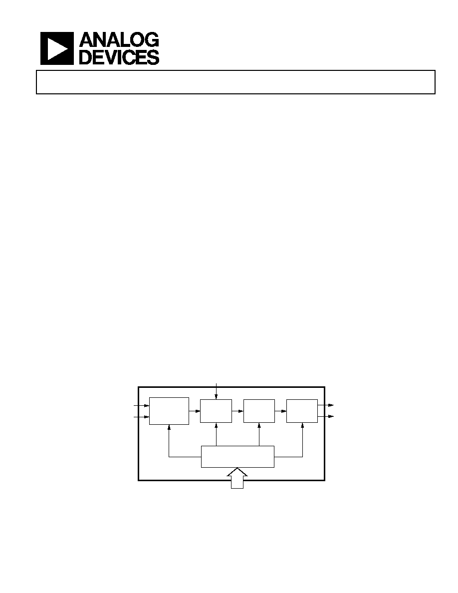
BASIC BLOCK DIAGRAM
REFERENCE
CONDITIONING
AND SWITCH-
OVER
HOLDOVER
LOOP
PLL
OUTPUT
CIRCUITRY
PIN-DEFINED AND SERIAL
PROGRAMMING
REFA
CRYSTAL
(26MHz)
REFB
OUT1
OUT2
AD9551
07
80
5-
0
01
Figure 1.
相关PDF资料 |
PDF描述 |
|---|---|
| AD9552BCPZ-REEL7 | IC PLL CLOCK GEN LP 32LFCSP |
| AD9553BCPZ-REEL7 | IC INTEGER-N CLCK GEN 32LFCSP |
| AD9557BCPZ-REEL7 | IC CLK XLATR PLL 1250MHZ 40LFCSP |
| AD9558BCPZ-REEL7 | IC CLK XLATR PLL 1250MHZ 64LFCSP |
| AD9571ACPZPEC-R7 | IC PLL CLOCK GEN 25MHZ 40LFCSP |
相关代理商/技术参数 |
参数描述 |
|---|---|
| AD9551BCPZ-REEL7 | 功能描述:IC CLOCK GEN TRANSLATOR 40LFCSP RoHS:是 类别:集成电路 (IC) >> 时钟/计时 - 时钟发生器,PLL,频率合成器 系列:- 标准包装:2,000 系列:- 类型:PLL 时钟发生器 PLL:带旁路 输入:LVCMOS,LVPECL 输出:LVCMOS 电路数:1 比率 - 输入:输出:2:11 差分 - 输入:输出:是/无 频率 - 最大:240MHz 除法器/乘法器:是/无 电源电压:3.135 V ~ 3.465 V 工作温度:0°C ~ 70°C 安装类型:表面贴装 封装/外壳:32-LQFP 供应商设备封装:32-TQFP(7x7) 包装:带卷 (TR) |
| AD9552 | 制造商:AD 制造商全称:Analog Devices 功能描述:Oscillator Frequency Upconverter |
| AD9552/PCBZ | 功能描述:BOARD EVALUATION FOR AD9552 RoHS:是 类别:编程器,开发系统 >> 评估演示板和套件 系列:- 标准包装:1 系列:PSoC® 主要目的:电源管理,热管理 嵌入式:- 已用 IC / 零件:- 主要属性:- 次要属性:- 已供物品:板,CD,电源 |
| AD9552BCPZ | 功能描述:IC PLL CLOCK GEN LP 32LFCSP RoHS:是 类别:集成电路 (IC) >> 时钟/计时 - 时钟发生器,PLL,频率合成器 系列:- 标准包装:2,000 系列:- 类型:PLL 频率合成器 PLL:是 输入:晶体 输出:时钟 电路数:1 比率 - 输入:输出:1:1 差分 - 输入:输出:无/无 频率 - 最大:1GHz 除法器/乘法器:是/无 电源电压:4.5 V ~ 5.5 V 工作温度:-20°C ~ 85°C 安装类型:表面贴装 封装/外壳:16-LSSOP(0.175",4.40mm 宽) 供应商设备封装:16-SSOP 包装:带卷 (TR) 其它名称:NJW1504V-TE1-NDNJW1504V-TE1TR |
| AD9552BCPZ | 制造商:Analog Devices 功能描述:IC PLL CLOCK GENERATOR 112.5MHZ LFCSP-32 |
发布紧急采购,3分钟左右您将得到回复。