参数资料
| 型号: | AD9552BCPZ-REEL7 |
| 厂商: | Analog Devices Inc |
| 文件页数: | 14/32页 |
| 文件大小: | 0K |
| 描述: | IC PLL CLOCK GEN LP 32LFCSP |
| 设计资源: | Clock Distribution Circuit with Pin-Programmable Output Frequency, Output Logic Levels, and Fanout (CN0152) |
| 标准包装: | 1,500 |
| 类型: | 时钟发生器 |
| PLL: | 带旁路 |
| 输入: | 时钟,晶体 |
| 输出: | CMOS,LVDS,LVPECL |
| 电路数: | 1 |
| 比率 - 输入:输出: | 2:2 |
| 差分 - 输入:输出: | 无/是 |
| 频率 - 最大: | 900MHz |
| 除法器/乘法器: | 是/无 |
| 电源电压: | 3.3V |
| 工作温度: | -40°C ~ 85°C |
| 安装类型: | 表面贴装 |
| 封装/外壳: | 32-VFQFN 裸露焊盘,CSP |
| 供应商设备封装: | 32-LFCSP-VQ(5x5) |
| 包装: | 带卷 (TR) |
第1页第2页第3页第4页第5页第6页第7页第8页第9页第10页第11页第12页第13页当前第14页第15页第16页第17页第18页第19页第20页第21页第22页第23页第24页第25页第26页第27页第28页第29页第30页第31页第32页
Data Sheet
AD9552
Rev. E | Page 21 of 32
By default, a read request reads the register value that is currently
in use by the AD9552. However, setting Register 0x04[0] = 1
causes the buffered registers to be read instead. The buffered
registers are the ones that take effect during the next I/O update.
07806-
007
AD9552
CORE
CO
NT
RO
L
R
EG
IST
ER
S
SERIAL
CONTROL
PORT
RE
G
IS
T
E
R
BUF
F
E
RS
13
14
12
SCLK
SDIO
CS
EXECUTE AN
INPUT/OUTPUT
UPDATE
REGISTER
UPDATE
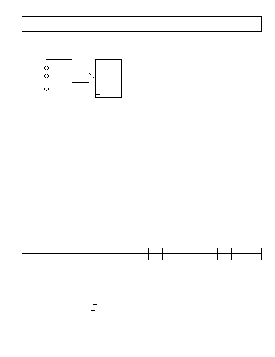
Figure 23. Relationship Between the Serial Control Port Register Buffers and
the Control Registers
The AD9552 uses Register 0x00 to Register 0x34. Although the
AD9552 serial control port allows both 8-bit and 16-bit instruc-
tions, the 8-bit instruction mode provides access to five address
bits (Address Bits[A4:A0]) only, which restricts its use to Address
Space 0x00 to Address Space 0x01. The AD9552 defaults to 16-bit
instruction mode on power-up, and the 8-bit instruction mode
is not supported.
INSTRUCTION WORD (16 BITS)
The MSB of the instruction word (see Table 15) is R/W, which
indicates whether the instruction is a read or a write. The next
two bits, W1 and W0, are the transfer length in bytes. The final
13 bits are the address bits (Address Bits[A12:A0]) at which the
read or write operation is to begin.
For a write, the instruction word is followed by the number of
bytes of data indicated by Bits[W1:W0], which is interpreted
according to Table 14.
Address Bits[A12:A0] select the address within the register map
that is written to or read from during the data transfer portion
of the communication cycle. The AD9552 uses all of the 13-bit
address space. For multibyte transfers, this address is the starting
byte address.
MSB/LSB FIRST TRANSFERS
The AD9552 instruction word and byte data can be MSB first or
LSB first. The default for the AD9552 is MSB first. The LSB first
mode can be set by writing a 1 to Register 0x00[6] and requires
that an I/O update be executed. Immediately after the LSB first
bit is set, all serial control port operations are changed to LSB
first order.
When MSB first mode is active, the instruction and data bytes
must be written from MSB to LSB. Multibyte data transfers in
MSB first format start with an instruction byte that includes the
register address of the most significant data byte. Subsequent
data bytes must follow in order from high address to low address.
In MSB first mode, the serial control port internal address gen-
erator decrements for each data byte of the multibyte transfer cycle.
When LSB first = 1 (LSB first), the instruction and data bytes
must be written from LSB to MSB. Multibyte data transfers
in LSB first format start with an instruction byte that includes
the register address of the least significant data byte followed
by multiple data bytes. The serial control port internal byte
address generator increments for each data byte of the multibyte
transfer cycle.
The AD9552 serial control port register address decrements from
the register address just written toward 0x00 for multibyte I/O
operations if the MSB first mode is active (default). If the LSB
first mode is active, the serial control port register address
increments from the address just written toward 0x34 for
multibyte I/O operations.
Unused addresses are not skipped during multibyte I/O operations.
The user should write the default value to a reserved register and
should write only zeros to unmapped registers. Note that it is more
efficient to issue a new write command than to write the default
value to more than two consecutive reserved (or unmapped)
registers.
Table 15. Serial Control Port, 16-Bit Instruction Word, MSB First
MSB
LSB
I15
I14
I13
I12
I11
I10
I9
I8
I7
I6
I5
I4
I3
I2
I1
I0
R/W
W1
W0
A12
A11
A10
A9
A8
A7
A6
A5
A4
A3
A2
A1
A0
Table 16. Definition of Terms Used in Serial Control Port Timing Diagrams
Parameter
Description
t
CLK
Period of SCLK
t
DV
Read data valid time (time from falling edge of SCLK to valid data on SDIO)
t
DS
Setup time between data and rising edge of SCLK
t
DH
Hold time between data and rising edge of SCLK
t
S
Setup time between CS and SCLK
t
H
Hold time between CS and SCLK
t
HIGH
Minimum period that SCLK should be in a logic high state
t
LOW
Minimum period that SCLK should be in a logic low state
相关PDF资料 |
PDF描述 |
|---|---|
| AD9553BCPZ-REEL7 | IC INTEGER-N CLCK GEN 32LFCSP |
| AD9557BCPZ-REEL7 | IC CLK XLATR PLL 1250MHZ 40LFCSP |
| AD9558BCPZ-REEL7 | IC CLK XLATR PLL 1250MHZ 64LFCSP |
| AD9571ACPZPEC-R7 | IC PLL CLOCK GEN 25MHZ 40LFCSP |
| AD9572ACPZLVD-R7 | IC PLL CLOCK GEN 25MHZ 40LFCSP |
相关代理商/技术参数 |
参数描述 |
|---|---|
| AD9552PCBZ | 制造商:AD 制造商全称:Analog Devices 功能描述:Oscillator Frequency Upconverter |
| AD9553 | 制造商:AD 制造商全称:Analog Devices 功能描述:Flexible Clock Translator for GPON, Base Station, SONET/SDH, T1/E1, and Ethernet |
| AD9553/PCBZ | 功能描述:BOARD EVAL FOR AD9553 RoHS:是 类别:编程器,开发系统 >> 评估演示板和套件 系列:- 标准包装:1 系列:- 主要目的:电信,线路接口单元(LIU) 嵌入式:- 已用 IC / 零件:IDT82V2081 主要属性:T1/J1/E1 LIU 次要属性:- 已供物品:板,电源,线缆,CD 其它名称:82EBV2081 |
| AD9553BCPZ | 功能描述:IC INTEGER-N CLCK GEN 32LFCSP RoHS:是 类别:集成电路 (IC) >> 时钟/计时 - 专用 系列:- 标准包装:1 系列:- 类型:时钟/频率发生器,多路复用器 PLL:是 主要目的:存储器,RDRAM 输入:晶体 输出:LVCMOS 电路数:1 比率 - 输入:输出:1:2 差分 - 输入:输出:无/是 频率 - 最大:400MHz 电源电压:3 V ~ 3.6 V 工作温度:0°C ~ 85°C 安装类型:表面贴装 封装/外壳:16-TSSOP(0.173",4.40mm 宽) 供应商设备封装:16-TSSOP 包装:Digi-Reel® 其它名称:296-6719-6 |
| AD9553BCPZ-REEL7 | 功能描述:IC INTEGER-N CLCK GEN 32LFCSP RoHS:是 类别:集成电路 (IC) >> 时钟/计时 - 专用 系列:- 标准包装:28 系列:- 类型:时钟/频率发生器 PLL:是 主要目的:Intel CPU 服务器 输入:时钟 输出:LVCMOS 电路数:1 比率 - 输入:输出:3:22 差分 - 输入:输出:无/是 频率 - 最大:400MHz 电源电压:3.135 V ~ 3.465 V 工作温度:0°C ~ 85°C 安装类型:表面贴装 封装/外壳:64-TFSOP (0.240",6.10mm 宽) 供应商设备封装:64-TSSOP 包装:管件 |
发布紧急采购,3分钟左右您将得到回复。