参数资料
| 型号: | AD9552BCPZ-REEL7 |
| 厂商: | Analog Devices Inc |
| 文件页数: | 5/32页 |
| 文件大小: | 0K |
| 描述: | IC PLL CLOCK GEN LP 32LFCSP |
| 设计资源: | Clock Distribution Circuit with Pin-Programmable Output Frequency, Output Logic Levels, and Fanout (CN0152) |
| 标准包装: | 1,500 |
| 类型: | 时钟发生器 |
| PLL: | 带旁路 |
| 输入: | 时钟,晶体 |
| 输出: | CMOS,LVDS,LVPECL |
| 电路数: | 1 |
| 比率 - 输入:输出: | 2:2 |
| 差分 - 输入:输出: | 无/是 |
| 频率 - 最大: | 900MHz |
| 除法器/乘法器: | 是/无 |
| 电源电压: | 3.3V |
| 工作温度: | -40°C ~ 85°C |
| 安装类型: | 表面贴装 |
| 封装/外壳: | 32-VFQFN 裸露焊盘,CSP |
| 供应商设备封装: | 32-LFCSP-VQ(5x5) |
| 包装: | 带卷 (TR) |
第1页第2页第3页第4页当前第5页第6页第7页第8页第9页第10页第11页第12页第13页第14页第15页第16页第17页第18页第19页第20页第21页第22页第23页第24页第25页第26页第27页第28页第29页第30页第31页第32页
Data Sheet
AD9552
Rev. E | Page 13 of 32
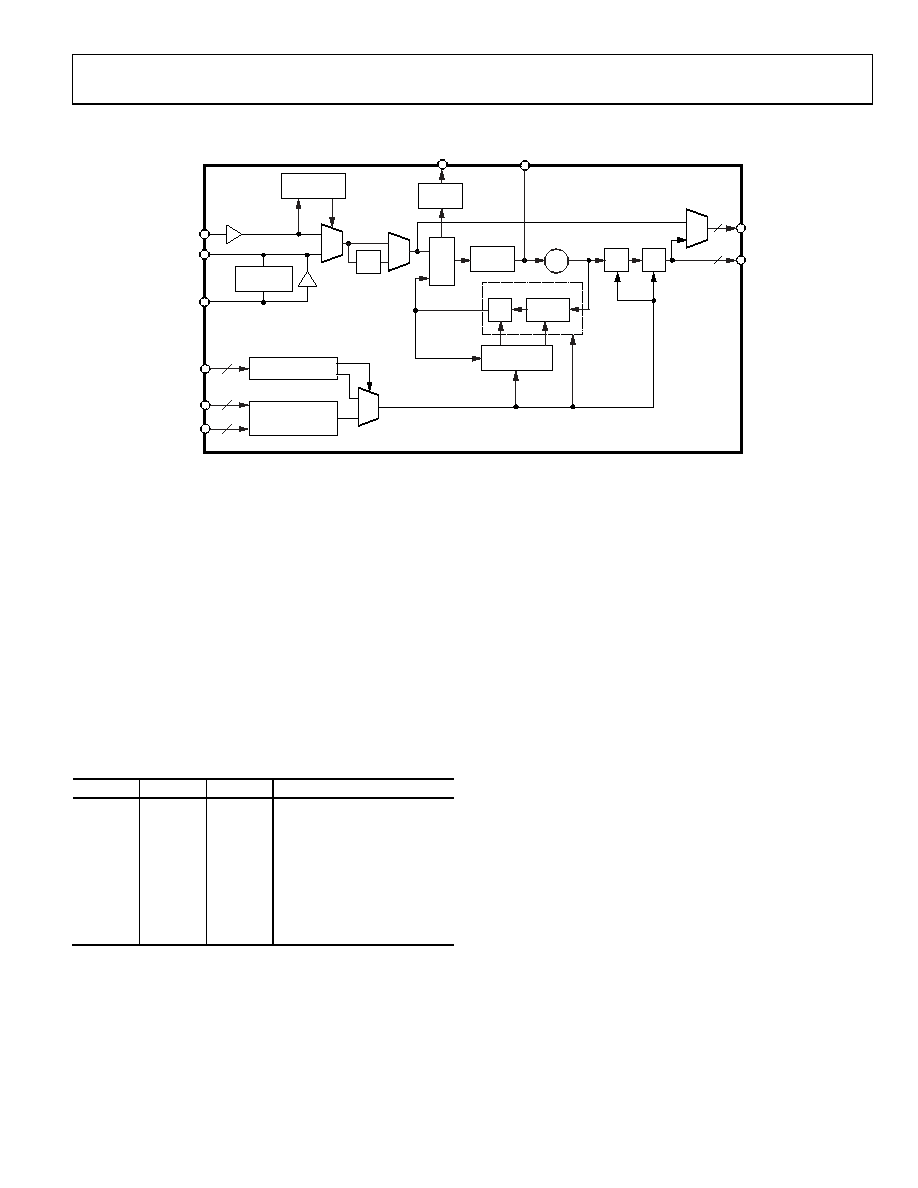
THEORY OF OPERATION
07806-
006
REFA
XTAL
SERIAL
PORT
A2:0
Y5:0
OUT2
FILTER
OUT1
REGISTER BANK
Σ-Δ
MODULATOR
PFD
CHARGE
PUMP
LOCK
DETECT
DETECTOR
PRECONFIGURED
DIVIDER VALUES
3
6
N, MOD, FRAC, P0, P1
AD9552
P0, P1
MOD,
FRAC
N
N1
P0
P1
4 OR 5
N = 4N1 + N0
2
4 TO 11
1 TO 63
3350MHz TO
4050MHz
VCO
LOCKED
TUNING
CONTROL
2×
Figure 19. Detailed Block Diagram
PRESET FREQUENCY RATIOS
The frequency selection pins (A[2:0] and Y[5:0]) allow the user
to hardwire the device for preset input and output divider values
based on the pin logic states (see Figure 19). The pins decode
ground or open connections as Logic 0 or Logic 1, respectively.
Use the serial I/O port to change the divider values from the
preset values provided by the A[2:0] and Y[5:0] pins.
The A[2:0] pins select one of eight input reference frequencies
(see Table 9). The user supplies the input reference frequency by
connecting a single-ended clock signal to the REF pin or a crystal
resonator across the XTAL pins. If the A[2:0] pins select 10 MHz,
12 MHz, 12.8 MHz, or 16 MHz, the input frequency to the AD9552
doubles internally. Alternatively, if Register 0x1D[2] is set to 1,
the input frequency doubles.
Table 9. Input Reference Frequency Selection Pins
A2
A1
A0
Reference Frequency (MHz)
0
10.00
0
1
12.00
0
1
0
12.80
0
1
16.00
1
0
19.20
1
0
1
19.44
1
0
20.00
1
26.00
The Y[5:0] pins select the appropriate feedback and output dividers
to synthesize the output frequencies (see Table 10). The output
frequencies provided in Table 10 are exact; that is, the number of
decimal places displayed is sufficient to maintain full precision.
Where a decimal representation is not practical, a fractional
multiplier is used.
The VCO and output frequency shift in frequency by a ratio of the
reference frequency used vs. the frequency specified in Table 9.
Note that the VCO frequency must stay within the minimum and
maximum range specified in Table 1. Typically, the selection of
the VCO frequency band, as well as the gain adjustment, by the
external pin strap occurs as part of the device’s automatic VCO
calibration process, which initiates at power up (or reset). If the
user changes the VCO frequency band via the SPI interface,
however, a forced VCO calibration should be initiated by first
enabling SPI control of the VCO calibration (Register 0x0E[2] = 1)
and then writing a 1 to the calibrate VCO bit (Register 0x0E[7]).
相关PDF资料 |
PDF描述 |
|---|---|
| AD9553BCPZ-REEL7 | IC INTEGER-N CLCK GEN 32LFCSP |
| AD9557BCPZ-REEL7 | IC CLK XLATR PLL 1250MHZ 40LFCSP |
| AD9558BCPZ-REEL7 | IC CLK XLATR PLL 1250MHZ 64LFCSP |
| AD9571ACPZPEC-R7 | IC PLL CLOCK GEN 25MHZ 40LFCSP |
| AD9572ACPZLVD-R7 | IC PLL CLOCK GEN 25MHZ 40LFCSP |
相关代理商/技术参数 |
参数描述 |
|---|---|
| AD9552PCBZ | 制造商:AD 制造商全称:Analog Devices 功能描述:Oscillator Frequency Upconverter |
| AD9553 | 制造商:AD 制造商全称:Analog Devices 功能描述:Flexible Clock Translator for GPON, Base Station, SONET/SDH, T1/E1, and Ethernet |
| AD9553/PCBZ | 功能描述:BOARD EVAL FOR AD9553 RoHS:是 类别:编程器,开发系统 >> 评估演示板和套件 系列:- 标准包装:1 系列:- 主要目的:电信,线路接口单元(LIU) 嵌入式:- 已用 IC / 零件:IDT82V2081 主要属性:T1/J1/E1 LIU 次要属性:- 已供物品:板,电源,线缆,CD 其它名称:82EBV2081 |
| AD9553BCPZ | 功能描述:IC INTEGER-N CLCK GEN 32LFCSP RoHS:是 类别:集成电路 (IC) >> 时钟/计时 - 专用 系列:- 标准包装:1 系列:- 类型:时钟/频率发生器,多路复用器 PLL:是 主要目的:存储器,RDRAM 输入:晶体 输出:LVCMOS 电路数:1 比率 - 输入:输出:1:2 差分 - 输入:输出:无/是 频率 - 最大:400MHz 电源电压:3 V ~ 3.6 V 工作温度:0°C ~ 85°C 安装类型:表面贴装 封装/外壳:16-TSSOP(0.173",4.40mm 宽) 供应商设备封装:16-TSSOP 包装:Digi-Reel® 其它名称:296-6719-6 |
| AD9553BCPZ-REEL7 | 功能描述:IC INTEGER-N CLCK GEN 32LFCSP RoHS:是 类别:集成电路 (IC) >> 时钟/计时 - 专用 系列:- 标准包装:28 系列:- 类型:时钟/频率发生器 PLL:是 主要目的:Intel CPU 服务器 输入:时钟 输出:LVCMOS 电路数:1 比率 - 输入:输出:3:22 差分 - 输入:输出:无/是 频率 - 最大:400MHz 电源电压:3.135 V ~ 3.465 V 工作温度:0°C ~ 85°C 安装类型:表面贴装 封装/外壳:64-TFSOP (0.240",6.10mm 宽) 供应商设备封装:64-TSSOP 包装:管件 |
发布紧急采购,3分钟左右您将得到回复。