参数资料
| 型号: | AD9552BCPZ-REEL7 |
| 厂商: | Analog Devices Inc |
| 文件页数: | 7/32页 |
| 文件大小: | 0K |
| 描述: | IC PLL CLOCK GEN LP 32LFCSP |
| 设计资源: | Clock Distribution Circuit with Pin-Programmable Output Frequency, Output Logic Levels, and Fanout (CN0152) |
| 标准包装: | 1,500 |
| 类型: | 时钟发生器 |
| PLL: | 带旁路 |
| 输入: | 时钟,晶体 |
| 输出: | CMOS,LVDS,LVPECL |
| 电路数: | 1 |
| 比率 - 输入:输出: | 2:2 |
| 差分 - 输入:输出: | 无/是 |
| 频率 - 最大: | 900MHz |
| 除法器/乘法器: | 是/无 |
| 电源电压: | 3.3V |
| 工作温度: | -40°C ~ 85°C |
| 安装类型: | 表面贴装 |
| 封装/外壳: | 32-VFQFN 裸露焊盘,CSP |
| 供应商设备封装: | 32-LFCSP-VQ(5x5) |
| 包装: | 带卷 (TR) |
第1页第2页第3页第4页第5页第6页当前第7页第8页第9页第10页第11页第12页第13页第14页第15页第16页第17页第18页第19页第20页第21页第22页第23页第24页第25页第26页第27页第28页第29页第30页第31页第32页
Data Sheet
AD9552
Rev. E | Page 15 of 32
Y5
Y4
Y3
Y2
Y1
Y0
VCO Frequency (MHz)
Output (MHz)
1
0
1
0
3536.763
657.421875 × (255/237)
1
0
1
3582.686
716.5372
1
0
3593.75
718.75
1
0
1
3598.672
719.7344
1
0
1
0
3740.355
748.0709
1
0
1
3750
750
1
0
3888
777.6
1
0
1
3897.843
779.5686
1
0
3906.25
781.25
1
4028.32
625 × (10/8) × (66/64)
COMPONENT BLOCKS
Input Reference
The AD9552 offers the following input reference options:
Crystal resonator connected directly across the XTAL pins
CMOS-compatible, single-ended clock source connected
directly to the REF pin
In the case of a crystal resonator, the AD9552 expects a crystal
with a specified load capacitance of 15 pF (default). The
AD9552 provides the load capacitance internally. The internal
load capacitance consists of a fixed component of 13 pF and a
variable (programmable) component of 0 pF to 15.75 pF.
After applying power to the AD9552 (or after a device reset),
the programmable component assumes a value of 2 pF. This
establishes the default load capacitance of 15 pF.
To accommodate crystals with a specified load capacitance other
than 15 pF (8 pF to 23.75 pF), the user can adjust the program-
mable capacitance in 0.25 pF increments via Register 0x1B[5:0].
Note that when the user sets Register 0x1B[7] to 0 (enabling SPI
control of the XTAL tuning capacitors), the variable capacitance
changes from 2 pF (its power-up value) to 15.75 pF due to the
default value of Register 0x1B[5:0]. This causes the crystal load
capacitance to be 23.75 pF until the user overwrites the default
contents of Register 0x1B[5:0].
A noncomprehensive, alphabetical list of crystal manufacturers
includes the following:
AVX/Kyocera
ECS
Epson Toyocom
Fox Electronics
NDK
Siward
The AD9552 evaluation board functions with the NDK
NX3225SA crystal or with the Siward 571200-A258-001 crystal.
Although these crystals meet the load capacitance and motional
resistance requirements of the AD9552 according to their data
sheets, Analog Devices, Inc., does not guarantee their operation
with the AD9552, nor does Analog Devices endorse one supplier
of crystals over another.
Reference Monitor
The REF input includes a monitor circuit that detects signal
presence at the REF input. If the device detects a clock signal on
the REF pin, it automatically selects the REF input as the input
reference source and shuts down the crystal oscillator. This auto-
matic preference for a REF input signal is the default mode of
operation. However, the user can override the default setting via
Register 0x1D[0]. Setting this bit forces the device to override the
signal detector associated with the REF input and activates the
crystal oscillator (whether or not a REF input signal is present).
2× Frequency Multiplier
The 2× frequency multiplier provides the option to double
the frequency delivered by either the REF or XTAL input. This
allows the user to take advantage of a higher frequency deli-
vered to the PLL, which allows for greater separation between
the frequency generated by the PLL and the associated reference
spur. However, increased reference spur separation comes at the
expense of the harmonic spurs introduced by the frequency
multiplier. As such, beneficial use of the frequency multiplier
is application specific.
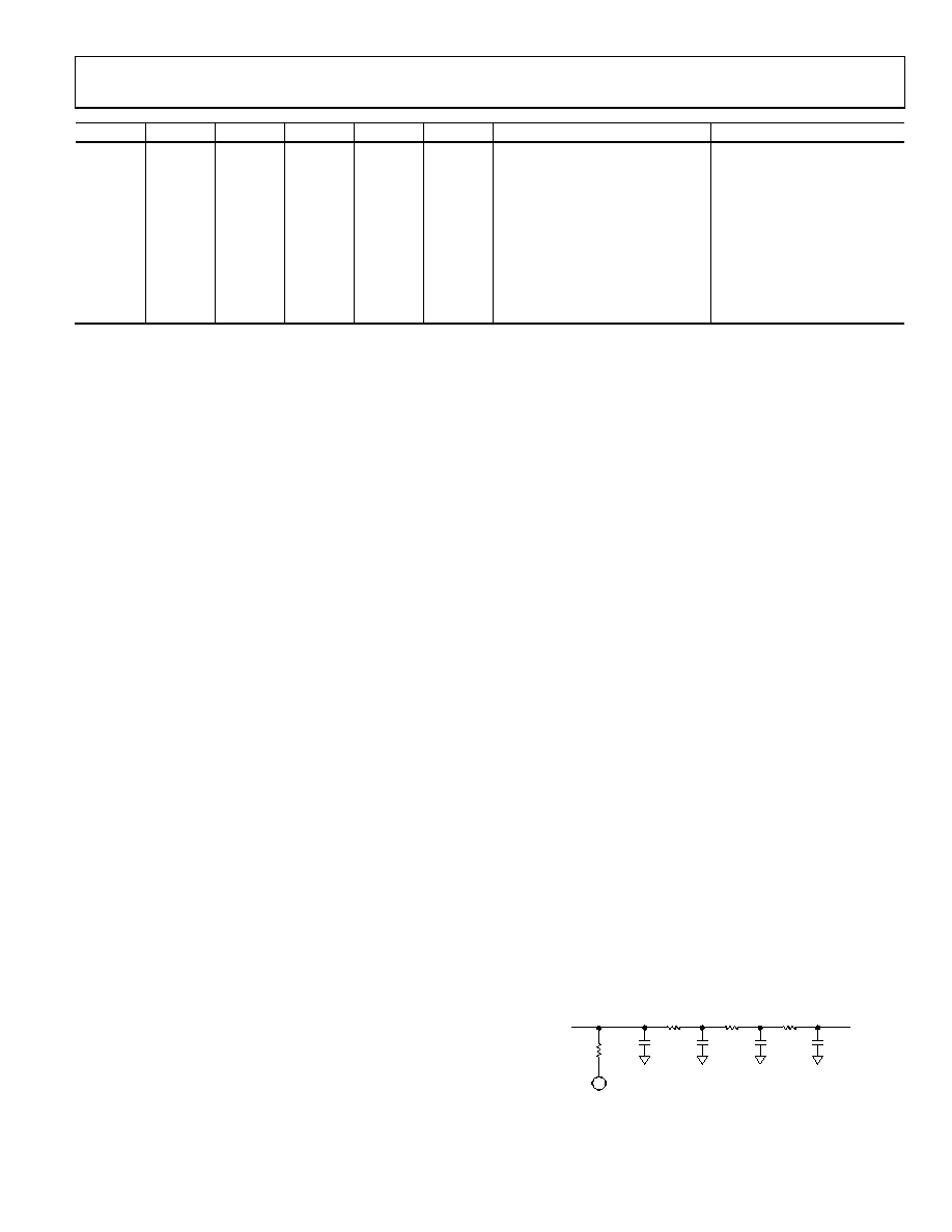
PLL
The PLL consists of a phase/frequency detector (PFD), a
partially integrated analog loop filter (see Figure 20), an
integrated voltage-controlled oscillator (VCO), and a
feedback divider with an optional third-order SDM that
allows for fractional divide ratios. The PLL produces a
nominal 3.7 GHz signal that is phase-locked to the input
reference signal.
The loop bandwidth of the PLL is nominally 50 kHz. The PFD of
the PLL drives a charge pump that automatically changes current
proportionately to the feedback divider value. This increase or
decrease in current maintains a constant loop bandwidth with
changes in the input reference or the output frequency.
16
EXTERNAL
LOOP FILTER
CAPACITOR
2.5k
1.25k
2.5k
105pF
15pF
20pF
FROM
CHARGE
PUMP
TO
VCO
07806-
004
Figure 20. Internal Loop Filter
相关PDF资料 |
PDF描述 |
|---|---|
| AD9553BCPZ-REEL7 | IC INTEGER-N CLCK GEN 32LFCSP |
| AD9557BCPZ-REEL7 | IC CLK XLATR PLL 1250MHZ 40LFCSP |
| AD9558BCPZ-REEL7 | IC CLK XLATR PLL 1250MHZ 64LFCSP |
| AD9571ACPZPEC-R7 | IC PLL CLOCK GEN 25MHZ 40LFCSP |
| AD9572ACPZLVD-R7 | IC PLL CLOCK GEN 25MHZ 40LFCSP |
相关代理商/技术参数 |
参数描述 |
|---|---|
| AD9552PCBZ | 制造商:AD 制造商全称:Analog Devices 功能描述:Oscillator Frequency Upconverter |
| AD9553 | 制造商:AD 制造商全称:Analog Devices 功能描述:Flexible Clock Translator for GPON, Base Station, SONET/SDH, T1/E1, and Ethernet |
| AD9553/PCBZ | 功能描述:BOARD EVAL FOR AD9553 RoHS:是 类别:编程器,开发系统 >> 评估演示板和套件 系列:- 标准包装:1 系列:- 主要目的:电信,线路接口单元(LIU) 嵌入式:- 已用 IC / 零件:IDT82V2081 主要属性:T1/J1/E1 LIU 次要属性:- 已供物品:板,电源,线缆,CD 其它名称:82EBV2081 |
| AD9553BCPZ | 功能描述:IC INTEGER-N CLCK GEN 32LFCSP RoHS:是 类别:集成电路 (IC) >> 时钟/计时 - 专用 系列:- 标准包装:1 系列:- 类型:时钟/频率发生器,多路复用器 PLL:是 主要目的:存储器,RDRAM 输入:晶体 输出:LVCMOS 电路数:1 比率 - 输入:输出:1:2 差分 - 输入:输出:无/是 频率 - 最大:400MHz 电源电压:3 V ~ 3.6 V 工作温度:0°C ~ 85°C 安装类型:表面贴装 封装/外壳:16-TSSOP(0.173",4.40mm 宽) 供应商设备封装:16-TSSOP 包装:Digi-Reel® 其它名称:296-6719-6 |
| AD9553BCPZ-REEL7 | 功能描述:IC INTEGER-N CLCK GEN 32LFCSP RoHS:是 类别:集成电路 (IC) >> 时钟/计时 - 专用 系列:- 标准包装:28 系列:- 类型:时钟/频率发生器 PLL:是 主要目的:Intel CPU 服务器 输入:时钟 输出:LVCMOS 电路数:1 比率 - 输入:输出:3:22 差分 - 输入:输出:无/是 频率 - 最大:400MHz 电源电压:3.135 V ~ 3.465 V 工作温度:0°C ~ 85°C 安装类型:表面贴装 封装/外壳:64-TFSOP (0.240",6.10mm 宽) 供应商设备封装:64-TSSOP 包装:管件 |
发布紧急采购,3分钟左右您将得到回复。