- 您现在的位置:买卖IC网 > PDF目录17022 > AD9633-125EBZ (Analog Devices Inc)BOARD EVAL FOR AD9633 PDF资料下载
参数资料
| 型号: | AD9633-125EBZ |
| 厂商: | Analog Devices Inc |
| 文件页数: | 21/40页 |
| 文件大小: | 0K |
| 描述: | BOARD EVAL FOR AD9633 |
| 标准包装: | 1 |
| 系列: | * |
第1页第2页第3页第4页第5页第6页第7页第8页第9页第10页第11页第12页第13页第14页第15页第16页第17页第18页第19页第20页当前第21页第22页第23页第24页第25页第26页第27页第28页第29页第30页第31页第32页第33页第34页第35页第36页第37页第38页第39页第40页
AD9633
Data Sheet
Rev. 0 | Page 28 of 40
400
600
–400
–600
–200
200
0
–1ns
–0.5ns
0ns
0.5ns
1ns
EYE
D
IA
G
R
A
M
VO
L
T
A
G
E
(
m
V)
EYE: ALL BITS
ULS: 7000/301593
12k
10k
1k
2k
3k
4k
5k
6k
7k
8k
9k
0
–1ns –0.8ns –0.6ns –0.4ns –0.2ns 0ns
0.2ns 0.4ns
0.8ns
0.6ns
T
IE
JI
T
ER
H
IST
O
G
R
A
M
(H
it
s)
100
73
-076
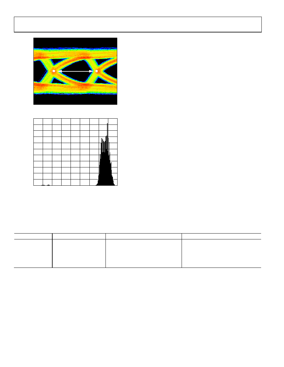
Figure 72 shows an example of trace lengths exceeding 24 inches
on standard FR-4 material. Notice that the TIE jitter histogram
reflects the decrease of the data eye opening as the edge deviates
from the ideal position. It is the user’s responsibility to determine
if the waveforms meet the timing budget of the design when the
trace lengths exceed 24 inches. Additional SPI options allow the
user to further increase the internal termination (increasing the
current) of all four outputs to drive longer trace lengths. This can
be achieved by programming Register 0x15. Even though this
produces sharper rise and fall times on the data edges and is less
prone to bit errors, the power dissipation of the DRVDD supply
increases when this option is used.
The format of the output data is twos complement by default.
An example of the output coding format can be found in Table 10.
To change the output data format to offset binary, see the
Memory Map section.
Data from each ADC is serialized and provided on a separate
channel in two lanes in DDR mode. The data rate for each serial
stream is equal to 12 bits times the sample clock rate, with a
maximum of 375 Mbps/lane [(12 bits × 125 MSPS)/(2 × 2) =
375 Mbps/lane)]. The lowest typical conversion rate is 10 MSPS.
See the Memory Map section for details on enabling this feature.
Two output clocks are provided to assist in capturing data from
the AD9633. The DCO is used to clock the output data and is
equal to three times the sample clock (CLK) rate for the default
mode of operation. Data is clocked out of the AD9633 and must
be captured on the rising and falling edges of the DCO that
supports double data rate (DDR) capturing. The FCO is used to
signal the start of a new output byte and is equal to the sample
clock rate in 1× frame mode. See the Timing Diagrams section for
more information.
Figure 72. Data Eye for LVDS Outputs in ANSI-644 Mode with Trace Lengths
Greater than 24 Inches on Standard FR-4 Material, External 100 Ω Far-End
Termination Only
Table 10. Digital Output Coding
Input (V)
Condition (V)
Offset Binary Output Mode
Twos Complement Mode
VIN+ VIN
<VREF 0.5 LSB
0000 0000 0000
1000 0000 0000
VIN+ VIN
VREF
0000 0000 0000
1000 0000 0000
VIN+ VIN
0 V
1000 0000 0000
0000 0000 0000
VIN+ VIN
+VREF 1.0 LSB
1111 1111 1111
0111 1111 1111
VIN+ VIN
>+VREF 0.5 LSB
1111 1111 1111
0111 1111 1111
相关PDF资料 |
PDF描述 |
|---|---|
| PM0805-68NK-RC | INDUCTOR CHIP 68NH 10% SMD |
| MAX1379EVKIT+ | EVAL KIT FOR MAX1379 |
| AD9608-125EBZ | BOARD EVAL AD9608-125 |
| AD9484-500EBZ | BOARD EVAL W/AD9484BCPZ-500 |
| SRR6038-560Y | INDUCTOR POWER 56UH .85A SMD |
相关代理商/技术参数 |
参数描述 |
|---|---|
| AD9633BCPZ-105 | 功能描述:IC ADC 12BIT SRL 105MSPS 48LFCSP RoHS:是 类别:集成电路 (IC) >> 数据采集 - 模数转换器 系列:- 其它有关文件:TSA1204 View All Specifications 标准包装:1 系列:- 位数:12 采样率(每秒):20M 数据接口:并联 转换器数目:2 功率耗散(最大):155mW 电压电源:模拟和数字 工作温度:-40°C ~ 85°C 安装类型:表面贴装 封装/外壳:48-TQFP 供应商设备封装:48-TQFP(7x7) 包装:Digi-Reel® 输入数目和类型:4 个单端,单极;2 个差分,单极 产品目录页面:1156 (CN2011-ZH PDF) 其它名称:497-5435-6 |
| AD9633BCPZ-125 | 功能描述:IC ADC 12BIT SRL 125MSPS 48LFCSP RoHS:是 类别:集成电路 (IC) >> 数据采集 - 模数转换器 系列:- 其它有关文件:TSA1204 View All Specifications 标准包装:1 系列:- 位数:12 采样率(每秒):20M 数据接口:并联 转换器数目:2 功率耗散(最大):155mW 电压电源:模拟和数字 工作温度:-40°C ~ 85°C 安装类型:表面贴装 封装/外壳:48-TQFP 供应商设备封装:48-TQFP(7x7) 包装:Digi-Reel® 输入数目和类型:4 个单端,单极;2 个差分,单极 产品目录页面:1156 (CN2011-ZH PDF) 其它名称:497-5435-6 |
| AD9633BCPZ-80 | 功能描述:IC ADC 12BIT SRL 80MSPS 48LFCSP RoHS:是 类别:集成电路 (IC) >> 数据采集 - 模数转换器 系列:- 其它有关文件:TSA1204 View All Specifications 标准包装:1 系列:- 位数:12 采样率(每秒):20M 数据接口:并联 转换器数目:2 功率耗散(最大):155mW 电压电源:模拟和数字 工作温度:-40°C ~ 85°C 安装类型:表面贴装 封装/外壳:48-TQFP 供应商设备封装:48-TQFP(7x7) 包装:Digi-Reel® 输入数目和类型:4 个单端,单极;2 个差分,单极 产品目录页面:1156 (CN2011-ZH PDF) 其它名称:497-5435-6 |
| AD9633BCPZRL7-105 | 功能描述:IC ADC 12BIT SRL 105MSPS 48LFCSP RoHS:是 类别:集成电路 (IC) >> 数据采集 - 模数转换器 系列:- 标准包装:1 系列:- 位数:14 采样率(每秒):83k 数据接口:串行,并联 转换器数目:1 功率耗散(最大):95mW 电压电源:双 ± 工作温度:0°C ~ 70°C 安装类型:通孔 封装/外壳:28-DIP(0.600",15.24mm) 供应商设备封装:28-PDIP 包装:管件 输入数目和类型:1 个单端,双极 |
| AD9633BCPZRL7-125 | 功能描述:模数转换器 - ADC 12 bit 125msps low pwr quad ADC RoHS:否 制造商:Analog Devices 通道数量: 结构: 转换速率: 分辨率: 输入类型: 信噪比: 接口类型: 工作电源电压: 最大工作温度: 安装风格: 封装 / 箱体: |
发布紧急采购,3分钟左右您将得到回复。