- 您现在的位置:买卖IC网 > PDF目录17022 > AD9633-125EBZ (Analog Devices Inc)BOARD EVAL FOR AD9633 PDF资料下载
参数资料
| 型号: | AD9633-125EBZ |
| 厂商: | Analog Devices Inc |
| 文件页数: | 33/40页 |
| 文件大小: | 0K |
| 描述: | BOARD EVAL FOR AD9633 |
| 标准包装: | 1 |
| 系列: | * |
第1页第2页第3页第4页第5页第6页第7页第8页第9页第10页第11页第12页第13页第14页第15页第16页第17页第18页第19页第20页第21页第22页第23页第24页第25页第26页第27页第28页第29页第30页第31页第32页当前第33页第34页第35页第36页第37页第38页第39页第40页
Data Sheet
AD9633
Rev. 0 | Page 39 of 40
APPLICATIONS INFORMATION
DESIGN GUIDELINES
Before starting design and layout of the AD9633 as a system,
it is recommended that the designer become familiar with these
guidelines, which describes the special circuit connections and
layout requirements that are needed for certain pins.
POWER AND GROUND RECOMMENDATIONS
When connecting power to the AD9633, it is recommended
that two separate 1.8 V supplies be used. Use one supply for
analog (AVDD); use a separate supply for the digital outputs
(DRVDD). For both AVDD and DRVDD, several different
decoupling capacitors should be used to cover both high and
low frequencies. Place these capacitors close to the point of
entry at the PCB level and close to the pins of the part, with
minimal trace length.
A single PCB ground plane should be sufficient when using the
AD9633. With proper decoupling and smart partitioning of the
PCB analog, digital, and clock sections, optimum performance
is easily achieved.
EXPOSED PAD THERMAL HEAT SLUG
RECOMMENDATIONS
It is required that the exposed pad on the underside of the ADC
be connected to analog ground (AGND) to achieve the best
electrical and thermal performance of the AD9633. An exposed
continuous copper plane on the PCB should mate to the
AD9633 exposed pad, Pin 0. The copper plane should have
several vias to achieve the lowest possible resistive thermal path
for heat dissipation to flow through the bottom of the PCB.
These vias should be solder-filled or plugged.
To maximize the coverage and adhesion between the ADC and
PCB, partition the continuous copper plane by overlaying a
silkscreen on the PCB into several uniform sections. This provides
several tie points between the ADC and PCB during the reflow
process, whereas using one continuous plane with no partitions
only guarantees one tie point. See Figure 74 for a PCB layout
example. For detailed information on packaging and the PCB
layout of chip scale packages, see the AN-772 Application Note,
A Design and Manufacturing Guide for the Lead Frame Chip
Scale Package (LFCSP), at www.analog.com.
SILKSCREEN PARTITION
PIN 1 INDICATOR
1
0073-
0
80
Figure 74. Typical PCB Layout
VCM
The VCM pin should be decoupled to ground with a 0.1 μF
capacitor.
REFERENCE DECOUPLING
The VREF pin should be externally decoupled to ground with a
low ESR, 1.0 μF capacitor in parallel with a low ESR, 0.1 μF
ceramic capacitor.
SPI PORT
The SPI port should not be active during periods when the full
dynamic performance of the converter is required. Because the
SCLK, CSB, and SDIO signals are typically asynchronous to the
ADC clock, noise from these signals can degrade converter
performance. If the on-board SPI bus is used for other devices,
it may be necessary to provide buffers between this bus and the
AD9633 to keep these signals from transitioning at the con-
verter inputs during critical sampling periods.
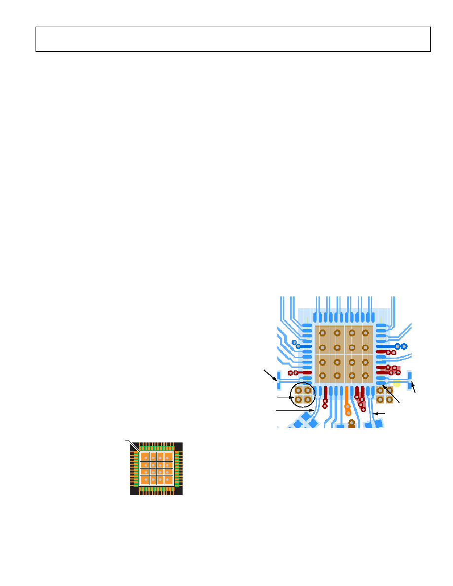
CROSSTALK PERFORMANCE
The AD9633 is available in a 48-lead LFCSP package with the
input pairs on either corner of the chip. See Figure 9 for the pin
configuration. To maximize the crosstalk performance on the
board, add grounded filled vias in between the adjacent
channels as shown in Figure 75.
GROUNDED
FILLED VIAS
FOR ADDED
CROSSTALK
ISOLATION
VIN
CHANNEL B
VIN
CHANNEL C
VIN
CHANNEL A
VIN
CHANNEL D
PIN 1
10
07
3
-08
8
Figure 75. Layout Technique to Maximize Crosstalk Performance
相关PDF资料 |
PDF描述 |
|---|---|
| PM0805-68NK-RC | INDUCTOR CHIP 68NH 10% SMD |
| MAX1379EVKIT+ | EVAL KIT FOR MAX1379 |
| AD9608-125EBZ | BOARD EVAL AD9608-125 |
| AD9484-500EBZ | BOARD EVAL W/AD9484BCPZ-500 |
| SRR6038-560Y | INDUCTOR POWER 56UH .85A SMD |
相关代理商/技术参数 |
参数描述 |
|---|---|
| AD9633BCPZ-105 | 功能描述:IC ADC 12BIT SRL 105MSPS 48LFCSP RoHS:是 类别:集成电路 (IC) >> 数据采集 - 模数转换器 系列:- 其它有关文件:TSA1204 View All Specifications 标准包装:1 系列:- 位数:12 采样率(每秒):20M 数据接口:并联 转换器数目:2 功率耗散(最大):155mW 电压电源:模拟和数字 工作温度:-40°C ~ 85°C 安装类型:表面贴装 封装/外壳:48-TQFP 供应商设备封装:48-TQFP(7x7) 包装:Digi-Reel® 输入数目和类型:4 个单端,单极;2 个差分,单极 产品目录页面:1156 (CN2011-ZH PDF) 其它名称:497-5435-6 |
| AD9633BCPZ-125 | 功能描述:IC ADC 12BIT SRL 125MSPS 48LFCSP RoHS:是 类别:集成电路 (IC) >> 数据采集 - 模数转换器 系列:- 其它有关文件:TSA1204 View All Specifications 标准包装:1 系列:- 位数:12 采样率(每秒):20M 数据接口:并联 转换器数目:2 功率耗散(最大):155mW 电压电源:模拟和数字 工作温度:-40°C ~ 85°C 安装类型:表面贴装 封装/外壳:48-TQFP 供应商设备封装:48-TQFP(7x7) 包装:Digi-Reel® 输入数目和类型:4 个单端,单极;2 个差分,单极 产品目录页面:1156 (CN2011-ZH PDF) 其它名称:497-5435-6 |
| AD9633BCPZ-80 | 功能描述:IC ADC 12BIT SRL 80MSPS 48LFCSP RoHS:是 类别:集成电路 (IC) >> 数据采集 - 模数转换器 系列:- 其它有关文件:TSA1204 View All Specifications 标准包装:1 系列:- 位数:12 采样率(每秒):20M 数据接口:并联 转换器数目:2 功率耗散(最大):155mW 电压电源:模拟和数字 工作温度:-40°C ~ 85°C 安装类型:表面贴装 封装/外壳:48-TQFP 供应商设备封装:48-TQFP(7x7) 包装:Digi-Reel® 输入数目和类型:4 个单端,单极;2 个差分,单极 产品目录页面:1156 (CN2011-ZH PDF) 其它名称:497-5435-6 |
| AD9633BCPZRL7-105 | 功能描述:IC ADC 12BIT SRL 105MSPS 48LFCSP RoHS:是 类别:集成电路 (IC) >> 数据采集 - 模数转换器 系列:- 标准包装:1 系列:- 位数:14 采样率(每秒):83k 数据接口:串行,并联 转换器数目:1 功率耗散(最大):95mW 电压电源:双 ± 工作温度:0°C ~ 70°C 安装类型:通孔 封装/外壳:28-DIP(0.600",15.24mm) 供应商设备封装:28-PDIP 包装:管件 输入数目和类型:1 个单端,双极 |
| AD9633BCPZRL7-125 | 功能描述:模数转换器 - ADC 12 bit 125msps low pwr quad ADC RoHS:否 制造商:Analog Devices 通道数量: 结构: 转换速率: 分辨率: 输入类型: 信噪比: 接口类型: 工作电源电压: 最大工作温度: 安装风格: 封装 / 箱体: |
发布紧急采购,3分钟左右您将得到回复。