- 您现在的位置:买卖IC网 > PDF目录10652 > AD9639BCPZ-210 (Analog Devices Inc)IC ADC 12B 170MSPS QUAD 72LFCSP PDF资料下载
参数资料
| 型号: | AD9639BCPZ-210 |
| 厂商: | Analog Devices Inc |
| 文件页数: | 11/36页 |
| 文件大小: | 0K |
| 描述: | IC ADC 12B 170MSPS QUAD 72LFCSP |
| 标准包装: | 1 |
| 位数: | 12 |
| 采样率(每秒): | 210M |
| 数据接口: | 串行,SPI? |
| 转换器数目: | 4 |
| 功率耗散(最大): | 1.22W |
| 电压电源: | 模拟和数字 |
| 工作温度: | -40°C ~ 85°C |
| 安装类型: | 表面贴装 |
| 封装/外壳: | 72-VFQFN 裸露焊盘,CSP |
| 供应商设备封装: | 72-LFCSP |
| 包装: | 托盘 |
| 输入数目和类型: | 8 个单端,单极;4 个差分,单极 |
第1页第2页第3页第4页第5页第6页第7页第8页第9页第10页当前第11页第12页第13页第14页第15页第16页第17页第18页第19页第20页第21页第22页第23页第24页第25页第26页第27页第28页第29页第30页第31页第32页第33页第34页第35页第36页
Data Sheet
AD9639
Rev. B | Page 19 of 36
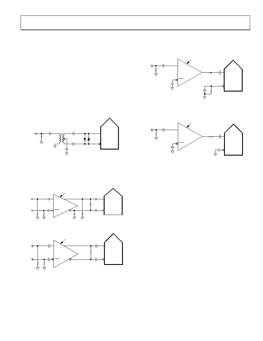
CLOCK INPUT CONSIDERATIONS
For optimum performance, the AD9639 sample clock inputs
(CLK+ and CLK) should be clocked with a differential signal.
This signal is typically ac-coupled to the CLK+ and CLK pins
via a transformer or capacitors. These pins are biased internally
to 1.2 V and require no additional biasing.
Figure 43 shows a preferred method for clocking the AD9639. The
low jitter clock source is converted from a single-ended signal
to a differential signal using an RF transformer. The back-to-
back Schottky diodes across the secondary transformer limit
clock excursions into the AD9639 to approximately 0.8 V p-p
differential. This helps to prevent the large voltage swings of the
clock from feeding through to other portions of the AD9639,
and it preserves the fast rise and fall times of the signal, which
are critical to low jitter performance.
0.1F
SCHOTTKY
DIODES:
HSMS-2812
CLK+
50
CLK–
CLK+
ADT1-1WT, 1:1Z
XFMR
ADC
AD9639
07973-
018
Figure 43. Transformer-Coupled Differential Clock
Another option is to ac-couple a differential PECL signal to the
sample clock input pins as shown in Figure 44. The AD9510/
family of clock drivers offers excellent jitter performance.
100
0.1F
240
240
50
*
50
*
CLK
CLK–
CLK+
ADC
AD9639
PECL DRIVER
CLK+
CLK–
AD9510/AD9511/
AD9512/AD9513/
AD9514/AD9515/
AD9516/AD9518
*50 RESISTORS ARE OPTIONAL.
07973-
019
Figure 44. Differential PECL Sample Clock
10
0
0.1F
50*
CLK
CLK–
CLK+
ADC
AD9639
LVDS DRIVER
CLK+
CLK–
AD9510/AD9511/
AD9512/AD9513/
AD9514/AD9515/
AD9516/AD9518
*50 RESISTORS ARE OPTIONAL.
07973-
020
Figure 45. Differential LVDS Sample Clock
In some applications, it is acceptable to drive the sample clock
inputs with a single-ended CMOS signal. In such applications,
CLK+ should be driven directly from a CMOS gate, and the
CLK pin should be bypassed to ground with a 0.1 μF capacitor
in parallel with a 39 k resistor (see Figure 46). Although the
CLK+ input circuit supply is AVDD (1.8 V), this input is
designed to withstand input voltages of up to 3.3 V and,
therefore, offers several selections for the drive logic voltage.
0.1F
39
k
50
*
0.1F
CLK
CLK–
CLK+
ADC
AD9639
CMOS DRIVER
CLK+
AD9510/AD9511/
AD9512/AD9513/
AD9514/AD9515/
AD9516/AD9518
*50 RESISTOR IS OPTIONAL.
OPTIONAL
100
07973-
021
Figure 46. Single-Ended 1.8 V CMOS Sample Clock
0.1F
CLK
0.1F
CLK–
CLK+
ADC
AD9639
OPTIONAL
100
CMOS DRIVER
CLK+
AD9510/AD9511/
AD9512/AD9513/
AD9514/AD9515/
AD9516/AD9518
*50 RESISTOR IS OPTIONAL.
50
*
07973-
022
Figure 47. Single-Ended 3.3 V CMOS Sample Clock
Clock Duty Cycle Considerations
Typical high speed ADCs use both clock edges to generate a
variety of internal timing signals. As a result, these ADCs may
be sensitive to the clock duty cycle. Commonly, a 5% tolerance
is required on the clock duty cycle to maintain dynamic perfor-
mance characteristics.
The AD9639 contains a duty cycle stabilizer (DCS) that retimes
the nonsampling edge, providing an internal clock signal with a
nominal 50% duty cycle. This allows a wide range of clock input
duty cycles without affecting the performance of the AD9639.
When the DCS is on (default), noise and distortion performance
are nearly flat for a wide range of duty cycles. However, some
applications may require the DCS function to be off. If so, keep
in mind that the dynamic range performance may be affected
when operated in this mode. See the Memory Map section for
more details on using this feature.
Jitter in the rising edge of the input is an important concern,
and it is not reduced by the internal stabilization circuit. The
duty cycle control loop does not function for clock rates of less
than 50 MHz nominal. It is not recommended that this ADC
clock be dynamic in nature. Moving the clock around dynami-
cally requires long wait times for the back end serial capture to
retime and resynchronize to the receiving logic. This long time
constant far exceeds the time that it takes for the DCS and the
PLL to lock and stabilize. Only in rare applications would it be
necessary to disable the DCS circuitry in the clock register (see
Address 0x09 in Table 15). Keeping the DCS circuit enabled is
recommended to maximize ac performance.
相关PDF资料 |
PDF描述 |
|---|---|
| VI-211-IW-F1 | CONVERTER MOD DC/DC 12V 100W |
| AD9253BCPZ-125 | IC ADC 14BIT SRL 125MSPS 48LFCSP |
| LTC2284IUP#PBF | IC ADC DUAL 14BIT 105MSPS 64-QFN |
| VE-211-IW-F4 | CONVERTER MOD DC/DC 12V 100W |
| LTC2172IUKG-14#PBF | IC ADC 14BIT SER/PAR 65M 52-QFN |
相关代理商/技术参数 |
参数描述 |
|---|---|
| AD9639BCPZRL-170 | 功能描述:IC ADC 12B 170MSPS QUAD 72LFCSP RoHS:是 类别:集成电路 (IC) >> 数据采集 - 模数转换器 系列:- 产品培训模块:Lead (SnPb) Finish for COTS Obsolescence Mitigation Program 标准包装:250 系列:- 位数:12 采样率(每秒):1.8M 数据接口:并联 转换器数目:1 功率耗散(最大):1.82W 电压电源:模拟和数字 工作温度:-40°C ~ 85°C 安装类型:表面贴装 封装/外壳:48-LQFP 供应商设备封装:48-LQFP(7x7) 包装:管件 输入数目和类型:2 个单端,单极 |
| AD9639BCPZRL-210 | 功能描述:模数转换器 - ADC Quad 12 Bit 210 MSPS Seria 1.8V ADC RoHS:否 制造商:Analog Devices 通道数量: 结构: 转换速率: 分辨率: 输入类型: 信噪比: 接口类型: 工作电源电压: 最大工作温度: 安装风格: 封装 / 箱体: |
| AD9640 | 制造商:AD 制造商全称:Analog Devices 功能描述:14-Bit, 80/105/125/150 MSPS, 1.8 V Dual Analog-to-Digital Converter |
| AD9640/PCB | 制造商:AD 制造商全称:Analog Devices 功能描述:14-Bit, 80/105/125/150 MSPS, 1.8 V Dual Analog-to-Digital Converter |
| AD9640-105EBZ | 功能描述:ADC 14BIT 105MSPS DUAL 64-LFCSP RoHS:是 类别:编程器,开发系统 >> 评估板 - 模数转换器 (ADC) 系列:- 产品培训模块:Obsolescence Mitigation Program 标准包装:1 系列:- ADC 的数量:1 位数:12 采样率(每秒):94.4k 数据接口:USB 输入范围:±VREF/2 在以下条件下的电源(标准):- 工作温度:-40°C ~ 85°C 已用 IC / 零件:MAX11645 已供物品:板,软件 |
发布紧急采购,3分钟左右您将得到回复。