- 您现在的位置:买卖IC网 > PDF目录10652 > AD9639BCPZ-210 (Analog Devices Inc)IC ADC 12B 170MSPS QUAD 72LFCSP PDF资料下载
参数资料
| 型号: | AD9639BCPZ-210 |
| 厂商: | Analog Devices Inc |
| 文件页数: | 13/36页 |
| 文件大小: | 0K |
| 描述: | IC ADC 12B 170MSPS QUAD 72LFCSP |
| 标准包装: | 1 |
| 位数: | 12 |
| 采样率(每秒): | 210M |
| 数据接口: | 串行,SPI? |
| 转换器数目: | 4 |
| 功率耗散(最大): | 1.22W |
| 电压电源: | 模拟和数字 |
| 工作温度: | -40°C ~ 85°C |
| 安装类型: | 表面贴装 |
| 封装/外壳: | 72-VFQFN 裸露焊盘,CSP |
| 供应商设备封装: | 72-LFCSP |
| 包装: | 托盘 |
| 输入数目和类型: | 8 个单端,单极;4 个差分,单极 |
第1页第2页第3页第4页第5页第6页第7页第8页第9页第10页第11页第12页当前第13页第14页第15页第16页第17页第18页第19页第20页第21页第22页第23页第24页第25页第26页第27页第28页第29页第30页第31页第32页第33页第34页第35页第36页
AD9639
Data Sheet
Rev. B | Page 20 of 36
Clock Jitter Considerations
High speed, high resolution ADCs are sensitive to the quality of the
clock input. The degradation in SNR at a given input frequency (fA)
due only to aperture jitter (tJ) can be calculated as follows:
SNR Degradation = 20 × log 10(1/2 × π × fA × tJ)
In this equation, the rms aperture jitter represents the root mean
square of all jitter sources, including the clock input, analog input
signal, and ADC aperture jitter. IF undersampling applications
are particularly sensitive to jitter (see Figure 48).
The clock input should be treated as an analog signal in cases
where aperture jitter may affect the dynamic range of the AD9639.
Power supplies for clock drivers should be separated from the
ADC output driver supplies to avoid modulating the clock signal
with digital noise. Low jitter, crystal-controlled oscillators are
the best clock sources. If the clock is generated from another
type of source (by gating, dividing, or another method), it
should be retimed by the original clock during the last step.
Refer to the AN-501 Application Note, the AN-756 Application
Note, and the Analog Dialogue article, “Analog-to-Digital Converter
Clock Optimization: A Test Engineering Perspective” (Volume 42,
Number 2, February 2008) for in-depth information about jitter
performance as it relates to ADCs (visit www.analog.com).
1
10
100
1000
30
40
50
60
70
80
90
100
110
120
130
0.125 ps
0.25 ps
0.5 ps
1.0 ps
2.0 ps
RMS CLOCK JITTER REQUIREMENT
S
NR
(
d
B)
07973-
024
ANALOG INPUT FREQUENCY (MHz)
16 BITS
14 BITS
12 BITS
10 BITS
Figure 48. Ideal SNR vs. Input Frequency and Jitter
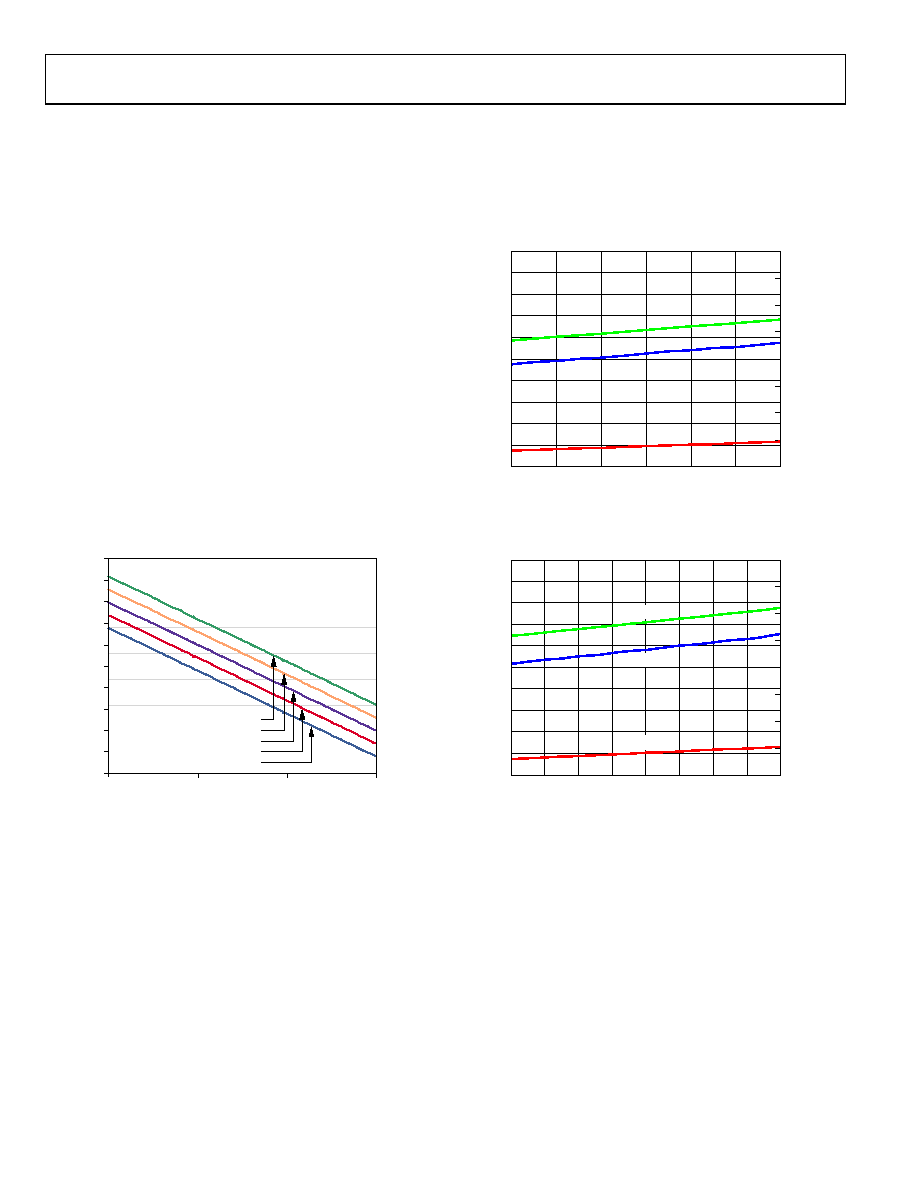
Power Dissipation
As shown in Figure 49 and Figure 50, the power dissipated by
the AD9639 is proportional to its clock rate. The digital power
dissipation does not vary significantly because it is determined
primarily by the DRVDD supply and the bias current of the
digital output drivers.
2.0
1.8
1.6
1.4
1.2
1.0
0.8
0.6
0.4
0.2
0
0.8
0.7
0.6
0.5
0.4
0.3
0.2
0.1
0
50
90
70
110
130
150
170
ENCODE (MSPS)
PO
W
ER
(W
)
CURRE
NT
(
mA)
IAVDD
POWER
IDRVDD
07973-
056
Figure 49. Supply Current vs. Encode for fIN = 84.3 MHz, fSAMPLE = 170 MSPS
2.0
1.8
1.6
1.4
1.2
1.0
0.8
0.6
0.4
0.2
0
0.8
0.7
0.6
0.5
0.4
0.3
0.2
0.1
0
50
90
70
110
130
150
170
190
210
ENCODE (MSPS)
PO
W
ER
(W
)
CURRE
NT
(
mA)
IAVDD
POWER
IDRVDD
07973-
057
Figure 50. Supply Current vs. Encode for fIN = 84.3 MHz, fSAMPLE = 210 MSPS
相关PDF资料 |
PDF描述 |
|---|---|
| VI-211-IW-F1 | CONVERTER MOD DC/DC 12V 100W |
| AD9253BCPZ-125 | IC ADC 14BIT SRL 125MSPS 48LFCSP |
| LTC2284IUP#PBF | IC ADC DUAL 14BIT 105MSPS 64-QFN |
| VE-211-IW-F4 | CONVERTER MOD DC/DC 12V 100W |
| LTC2172IUKG-14#PBF | IC ADC 14BIT SER/PAR 65M 52-QFN |
相关代理商/技术参数 |
参数描述 |
|---|---|
| AD9639BCPZRL-170 | 功能描述:IC ADC 12B 170MSPS QUAD 72LFCSP RoHS:是 类别:集成电路 (IC) >> 数据采集 - 模数转换器 系列:- 产品培训模块:Lead (SnPb) Finish for COTS Obsolescence Mitigation Program 标准包装:250 系列:- 位数:12 采样率(每秒):1.8M 数据接口:并联 转换器数目:1 功率耗散(最大):1.82W 电压电源:模拟和数字 工作温度:-40°C ~ 85°C 安装类型:表面贴装 封装/外壳:48-LQFP 供应商设备封装:48-LQFP(7x7) 包装:管件 输入数目和类型:2 个单端,单极 |
| AD9639BCPZRL-210 | 功能描述:模数转换器 - ADC Quad 12 Bit 210 MSPS Seria 1.8V ADC RoHS:否 制造商:Analog Devices 通道数量: 结构: 转换速率: 分辨率: 输入类型: 信噪比: 接口类型: 工作电源电压: 最大工作温度: 安装风格: 封装 / 箱体: |
| AD9640 | 制造商:AD 制造商全称:Analog Devices 功能描述:14-Bit, 80/105/125/150 MSPS, 1.8 V Dual Analog-to-Digital Converter |
| AD9640/PCB | 制造商:AD 制造商全称:Analog Devices 功能描述:14-Bit, 80/105/125/150 MSPS, 1.8 V Dual Analog-to-Digital Converter |
| AD9640-105EBZ | 功能描述:ADC 14BIT 105MSPS DUAL 64-LFCSP RoHS:是 类别:编程器,开发系统 >> 评估板 - 模数转换器 (ADC) 系列:- 产品培训模块:Obsolescence Mitigation Program 标准包装:1 系列:- ADC 的数量:1 位数:12 采样率(每秒):94.4k 数据接口:USB 输入范围:±VREF/2 在以下条件下的电源(标准):- 工作温度:-40°C ~ 85°C 已用 IC / 零件:MAX11645 已供物品:板,软件 |
发布紧急采购,3分钟左右您将得到回复。