- 您现在的位置:买卖IC网 > PDF目录17022 > AD9640-125EBZ (Analog Devices Inc)ADC 14BIT 125MSPS DUAL 64-LFCSP PDF资料下载
参数资料
| 型号: | AD9640-125EBZ |
| 厂商: | Analog Devices Inc |
| 文件页数: | 24/52页 |
| 文件大小: | 0K |
| 描述: | ADC 14BIT 125MSPS DUAL 64-LFCSP |
| 设计资源: | Interfacing ADL5534 to AD9640 High Speed ADC (CN0049) AD9640 Eval Brd Family Gerber Files AD9640 Eval Brd BOM AD9640 Eval Brd Schematic |
| 标准包装: | 1 |
| ADC 的数量: | 2 |
| 位数: | 14 |
| 采样率(每秒): | 125M |
| 数据接口: | 串行 |
| 输入范围: | 2 Vpp |
| 在以下条件下的电源(标准): | 910mW @ 125MSPS |
| 工作温度: | -40°C ~ 85°C |
| 已用 IC / 零件: | AD9640 |
| 已供物品: | 板 |
第1页第2页第3页第4页第5页第6页第7页第8页第9页第10页第11页第12页第13页第14页第15页第16页第17页第18页第19页第20页第21页第22页第23页当前第24页第25页第26页第27页第28页第29页第30页第31页第32页第33页第34页第35页第36页第37页第38页第39页第40页第41页第42页第43页第44页第45页第46页第47页第48页第49页第50页第51页第52页
AD9640
Rev. B | Page 30 of 52
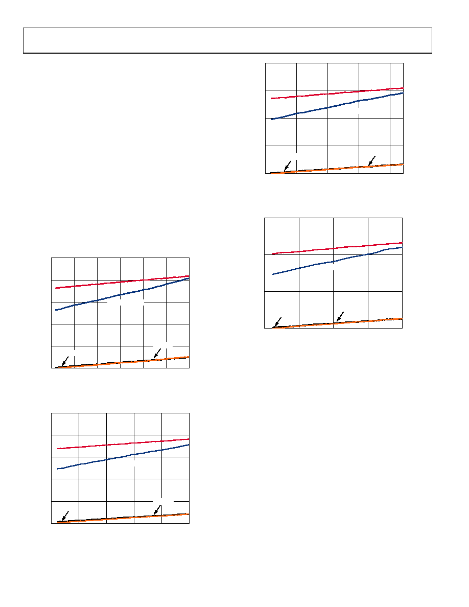
POWER DISSIPATION AND STANDBY MODE
As shown in Figure 63, the power dissipated by the AD9640
is proportional to its sample rate. In CMOS output mode,
the digital power dissipation is determined primarily by the
strength of the digital drivers and the load on each output bit.
The maximum DRVDD current (IDRVDD) can be calculated as
IDRVDD = VDRVDD × CLOAD × fCLK × N
where N is the number of output bits (30 in the case of the AD9640
with the FD bits disabled). This maximum current occurs when
every output bit switches on every clock cycle, that is, a full-
scale square wave at the Nyquist frequency of fCLK/2. In practice,
the DRVDD current is established by the average number of
output bits switching, which is determined by the sample rate
and the characteristics of the analog input signal.
Reducing the capacitive load presented to the output drivers can
minimize digital power consumption. The data in Figure 63 was
taken with the same operating conditions as the Typical
Performance Characteristics, with a 5 pF load on each output
driver.
0
150
125
1.25
0.75
1.0
0
0
654
7-
0
76
ENCODE FREQUENCY (MHz)
T
O
TA
L
P
O
WE
R
(
W
)
S
UP
P
L
Y
C
URRE
N
T
(
A)
0.5
0.25
0.5
0.4
0.3
0.2
0.1
0
25
50
75
100
IAVDD
TOTAL POWER
IDRVDD
IDVDD
Figure 63. AD9640-150 Power and Current vs. Clock Frequency
0
125
1.25
0.75
1.0
0
0
654
7-
0
75
ENCODE FREQUENCY (MHz)
T
O
TA
L
P
O
WE
R
(
W
)
S
UP
P
L
Y
CU
RRE
N
T
(
A)
0.5
0.25
0.5
0.4
0.3
0.2
0.1
0
25
50
75
100
IAVDD
TOTAL POWER
IDVDD
IDRVDD
Figure 64. AD9640-125 Power and Current vs. Clock Frequency
0
1
0
ENCODE FREQUENCY (MHz)
TOT
A
L
P
O
W
E
R
(W
)
0.75
0.25
0.5
25
50
75
100
06
54
7-
0
74
S
UP
P
L
Y
CURR
E
NT
(
A)
0.4
0.3
0.2
0.1
0
IAVDD
TOTAL POWER
IDRVDD
IDVDD
Figure 65. AD9640-105 Power and Current vs. Clock Frequency
08
0.75
0
0
654
7-
0
73
ENCODE FREQUENCY (MHz)
T
O
TA
L
P
O
WE
R
(
W
)
S
UP
P
L
Y
C
URRE
N
T
(
A)
0
0.5
0.25
0.3
0.2
0.1
0
20
40
60
IAVDD
TOTAL POWER
IDRVDD
IDVDD
Figure 66. AD9640-80 Power and Current vs. Clock Frequency
By asserting PDWN (either through the SPI port or by asserting
the PDWN pin high), the AD9640 is placed in power-down
mode. In this state, the ADC typically dissipates 2.5 mW.
During power-down, the output drivers are placed in a high
impedance state. Asserting the PDWN pin low returns the
AD9640 to its normal operational mode. Note that PDWN is
referenced to the digital supplies (DRVDD) and should not
exceed that supply voltage.
Low power dissipation in power-down mode is achieved by
shutting down the reference, reference buffer, biasing networks,
and clock. Internal capacitors are discharged when entering power-
down mode and then must be recharged when returning to normal
operation. As a result, wake-up time is related to the time spent
in power-down mode, and shorter power-down cycles result in
proportionally shorter wake-up times.
When using the SPI port interface, the user can place the ADC
in power-down mode or standby mode. Standby mode allows
the user to keep the internal reference circuitry powered when
faster wake-up times are required. See the Memory Map Register
Description section for more details.
相关PDF资料 |
PDF描述 |
|---|---|
| RCC15DRAH | CONN EDGECARD 30POS R/A .100 SLD |
| AD9640-105EBZ | ADC 14BIT 105MSPS DUAL 64-LFCSP |
| 1210-039M | INDUCTOR RF .0039UH MOLDED SMD |
| RBC18DCMI | CONN EDGECARD 36POS .100 WW |
| RCC17DCAI | CONN EDGECARD 34POS R/A .100 SLD |
相关代理商/技术参数 |
参数描述 |
|---|---|
| AD9640-150EBZ | 功能描述:数据转换 IC 开发工具 14Bit 150MspsDual 1.8V PB Free ADC RoHS:否 制造商:Texas Instruments 产品:Demonstration Kits 类型:ADC 工具用于评估:ADS130E08 接口类型:SPI 工作电源电压:- 6 V to + 6 V |
| AD9640-80EBZ | 功能描述:ADC 14BIT 80MSPS DUAL 64-LFCSP RoHS:是 类别:编程器,开发系统 >> 评估板 - 模数转换器 (ADC) 系列:- 产品培训模块:Obsolescence Mitigation Program 标准包装:1 系列:- ADC 的数量:1 位数:12 采样率(每秒):94.4k 数据接口:USB 输入范围:±VREF/2 在以下条件下的电源(标准):- 工作温度:-40°C ~ 85°C 已用 IC / 零件:MAX11645 已供物品:板,软件 |
| AD9640ABCPZ-105 | 功能描述:IC ADC 14BIT 105MSPS 64LFCSP RoHS:是 类别:集成电路 (IC) >> 数据采集 - 模数转换器 系列:- 产品培训模块:Lead (SnPb) Finish for COTS Obsolescence Mitigation Program 标准包装:250 系列:- 位数:12 采样率(每秒):1.8M 数据接口:并联 转换器数目:1 功率耗散(最大):1.82W 电压电源:模拟和数字 工作温度:-40°C ~ 85°C 安装类型:表面贴装 封装/外壳:48-LQFP 供应商设备封装:48-LQFP(7x7) 包装:管件 输入数目和类型:2 个单端,单极 |
| AD9640ABCPZ-125 | 功能描述:IC ADC 14BIT 125MSPS 64LFCSP RoHS:是 类别:集成电路 (IC) >> 数据采集 - 模数转换器 系列:- 产品培训模块:Lead (SnPb) Finish for COTS Obsolescence Mitigation Program 标准包装:250 系列:- 位数:12 采样率(每秒):1.8M 数据接口:并联 转换器数目:1 功率耗散(最大):1.82W 电压电源:模拟和数字 工作温度:-40°C ~ 85°C 安装类型:表面贴装 封装/外壳:48-LQFP 供应商设备封装:48-LQFP(7x7) 包装:管件 输入数目和类型:2 个单端,单极 |
| AD9640ABCPZ-150 | 功能描述:模数转换器 - ADC 14Bit 150Msps Dual 1.8V PB Free ADC RoHS:否 制造商:Analog Devices 通道数量: 结构: 转换速率: 分辨率: 输入类型: 信噪比: 接口类型: 工作电源电压: 最大工作温度: 安装风格: 封装 / 箱体: |
发布紧急采购,3分钟左右您将得到回复。