- 您现在的位置:买卖IC网 > PDF目录17022 > AD9640-125EBZ (Analog Devices Inc)ADC 14BIT 125MSPS DUAL 64-LFCSP PDF资料下载
参数资料
| 型号: | AD9640-125EBZ |
| 厂商: | Analog Devices Inc |
| 文件页数: | 30/52页 |
| 文件大小: | 0K |
| 描述: | ADC 14BIT 125MSPS DUAL 64-LFCSP |
| 设计资源: | Interfacing ADL5534 to AD9640 High Speed ADC (CN0049) AD9640 Eval Brd Family Gerber Files AD9640 Eval Brd BOM AD9640 Eval Brd Schematic |
| 标准包装: | 1 |
| ADC 的数量: | 2 |
| 位数: | 14 |
| 采样率(每秒): | 125M |
| 数据接口: | 串行 |
| 输入范围: | 2 Vpp |
| 在以下条件下的电源(标准): | 910mW @ 125MSPS |
| 工作温度: | -40°C ~ 85°C |
| 已用 IC / 零件: | AD9640 |
| 已供物品: | 板 |
第1页第2页第3页第4页第5页第6页第7页第8页第9页第10页第11页第12页第13页第14页第15页第16页第17页第18页第19页第20页第21页第22页第23页第24页第25页第26页第27页第28页第29页当前第30页第31页第32页第33页第34页第35页第36页第37页第38页第39页第40页第41页第42页第43页第44页第45页第46页第47页第48页第49页第50页第51页第52页
AD9640
Rev. B | Page 36 of 52
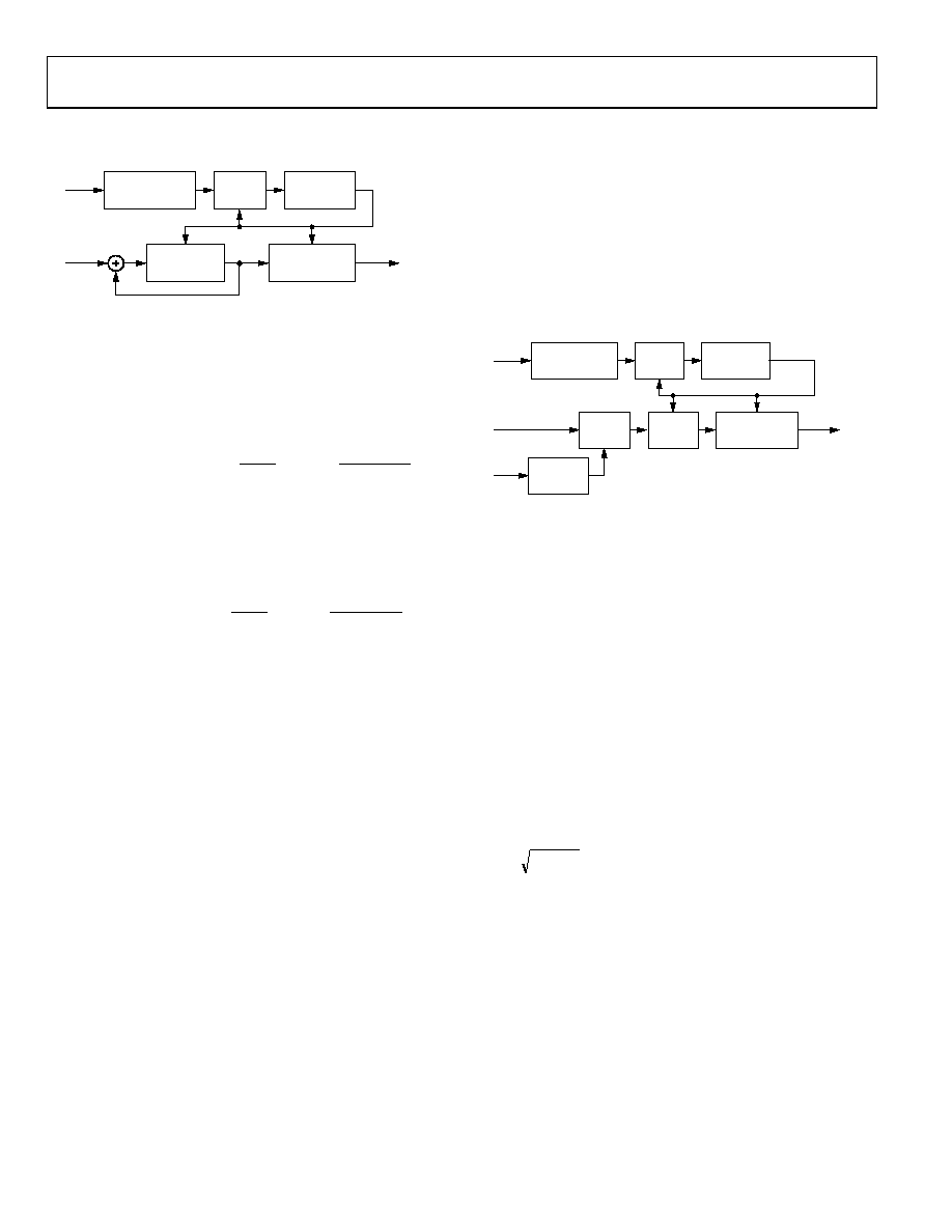
Figure 69 illustrates the rms magnitude monitoring logic.
SIGNAL MONITOR
HOLDING
REGISTER (SMR)
ACCUMULATOR
TO
MEMORY
MAP/SPORT
FROM
MEMORY
MAP
FROM
INPUT
PORTS
LOAD
CLEAR
LOAD
IS COUNT = 1?
DOWN
COUNTER
SIGNAL MONITOR
PERIOD REGISTER
06
54
7-
0
92
Figure 69. ADC Input RMS Magnitude Monitoring Block Diagram
For rms magnitude mode, the value in the signal monitor result
(SMR) register is a 20-bit fixed-point number. The following
equation can be used to determine the rms magnitude in dBFS
from the MAG value in the register. Note that if the signal monitor
period (SMP) is a power of 2, the second term in the equation
becomes 0.
RMS Magnitude = 20 log
[]
)
(
log
20
2
log
10
2
SMP
ceil
SMP
MAG
For ms magnitude mode, the value in the SMR is a 20-bit fixed-
point number. The following equation can be used to determine
the ms magnitude in dBFS from the MAG value in the register.
Note that if the SMP is a power of 2, the second term in the
equation becomes 0.
MS Magnitude = 10 log
[]
)
(
log
20
2
log
10
2
SMP
ceil
SMP
MAG
THRESHOLD CROSSING MODE
In the threshold crossing mode of operation, the magnitude of
the input port signal is monitored over a programmable time
period (given by the SMPR) to count the number of times it
crosses a certain programmable threshold value. This mode is set
by programming Logic 1x (where x is a don’t care bit) in the
signal monitor mode bits of the signal monitor control register
or by setting the threshold crossing output enable bit in the
signal monitor SPORT control register. Before activating this
mode, the user needs to program the 24-bit SMPR and the
13-bit upper threshold register for each individual input port.
The same upper threshold register is used for both signal moni-
toring and gain control (see the ADC Overrange and Gain
Control section).
After entering this mode, the value in the SMPR is loaded into
a monitor period timer, and the countdown is started. The magni-
tude of the input signal is compared with the upper threshold
register (programmed previously) on each input clock cycle.
If the input signal has a magnitude greater than the upper
threshold register, the internal count register is incremented by 1.
The initial value of the internal count register is set to 0. This
comparison and incrementing of the internal count register
continues until the monitor period timer reaches a count of 1.
When the monitor period timer reaches a count of 1, the value
in the internal count register is transferred to the signal monitor
holding register, which can be read through the SPI port or output
through the SPORT serial port.
The monitor period timer is reloaded with the value in the SMPR
register, and the countdown is restarted. The internal count
register is also cleared to a value of 0. Figure 70 illustrates the
threshold crossing logic. The value in the SMR register is the
number of samples that have a magnitude greater than the
threshold register.
SIGNAL MONITOR
HOLDING
REGISTER (SMR)
COMPARE
A>B
UPPER
THRESHOLD
REGISTER
COMPARE
A>B
TO
MEMORY
MAP/SPORT
FROM
MEMORY
MAP
FROM
MEMORY
MAP
FROM
INPUT
PORTS
LOAD
CLEAR
LOAD
IS COUNT = 1?
DOWN
COUNTER
SIGNAL MONITOR
PERIOD REGISTER
B
A
065
47
-04
6
Figure 70. ADC Input Threshold Crossing Block Diagram
ADDITIONAL CONTROL BITS
For additional flexibility in the signal monitoring process, two
control bits are provided in the signal monitor control register.
They are the signal monitor enable bit and the complex power
calculation mode enable bit.
Signal Monitor Enable Bit
The signal monitor enable bit, Bit 0 of Register 0x112, enables
operation of the signal monitor block. If the signal monitor
function is not needed in a particular application, this bit should
be cleared (default) to conserve power.
Complex Power Calculation Mode Enable Bit
When this bit is set, the part assumes that Channel A is digitizing
the I data and Channel B is digitizing the Q data for a complex
input signal (or vice versa). In this mode, the power reported is
equal to the following:
2
Q
I +
This result is presented in the Signal Monitor DC Value Channel A
register if the signal monitor mode bits are set to 00. The Signal
Monitor DC Value Channel B register continues to compute the
Channel B value.
DC CORRECTION
Because the dc offset of the ADC may be significantly larger
than the signal being measured, a dc correction circuit is included
to null the dc offset before measuring the power. The dc correction
circuit can also be switched into the main signal path, but this
may not be appropriate if the ADC is digitizing a time-varying
signal with significant dc content, such as GSM.
相关PDF资料 |
PDF描述 |
|---|---|
| RCC15DRAH | CONN EDGECARD 30POS R/A .100 SLD |
| AD9640-105EBZ | ADC 14BIT 105MSPS DUAL 64-LFCSP |
| 1210-039M | INDUCTOR RF .0039UH MOLDED SMD |
| RBC18DCMI | CONN EDGECARD 36POS .100 WW |
| RCC17DCAI | CONN EDGECARD 34POS R/A .100 SLD |
相关代理商/技术参数 |
参数描述 |
|---|---|
| AD9640-150EBZ | 功能描述:数据转换 IC 开发工具 14Bit 150MspsDual 1.8V PB Free ADC RoHS:否 制造商:Texas Instruments 产品:Demonstration Kits 类型:ADC 工具用于评估:ADS130E08 接口类型:SPI 工作电源电压:- 6 V to + 6 V |
| AD9640-80EBZ | 功能描述:ADC 14BIT 80MSPS DUAL 64-LFCSP RoHS:是 类别:编程器,开发系统 >> 评估板 - 模数转换器 (ADC) 系列:- 产品培训模块:Obsolescence Mitigation Program 标准包装:1 系列:- ADC 的数量:1 位数:12 采样率(每秒):94.4k 数据接口:USB 输入范围:±VREF/2 在以下条件下的电源(标准):- 工作温度:-40°C ~ 85°C 已用 IC / 零件:MAX11645 已供物品:板,软件 |
| AD9640ABCPZ-105 | 功能描述:IC ADC 14BIT 105MSPS 64LFCSP RoHS:是 类别:集成电路 (IC) >> 数据采集 - 模数转换器 系列:- 产品培训模块:Lead (SnPb) Finish for COTS Obsolescence Mitigation Program 标准包装:250 系列:- 位数:12 采样率(每秒):1.8M 数据接口:并联 转换器数目:1 功率耗散(最大):1.82W 电压电源:模拟和数字 工作温度:-40°C ~ 85°C 安装类型:表面贴装 封装/外壳:48-LQFP 供应商设备封装:48-LQFP(7x7) 包装:管件 输入数目和类型:2 个单端,单极 |
| AD9640ABCPZ-125 | 功能描述:IC ADC 14BIT 125MSPS 64LFCSP RoHS:是 类别:集成电路 (IC) >> 数据采集 - 模数转换器 系列:- 产品培训模块:Lead (SnPb) Finish for COTS Obsolescence Mitigation Program 标准包装:250 系列:- 位数:12 采样率(每秒):1.8M 数据接口:并联 转换器数目:1 功率耗散(最大):1.82W 电压电源:模拟和数字 工作温度:-40°C ~ 85°C 安装类型:表面贴装 封装/外壳:48-LQFP 供应商设备封装:48-LQFP(7x7) 包装:管件 输入数目和类型:2 个单端,单极 |
| AD9640ABCPZ-150 | 功能描述:模数转换器 - ADC 14Bit 150Msps Dual 1.8V PB Free ADC RoHS:否 制造商:Analog Devices 通道数量: 结构: 转换速率: 分辨率: 输入类型: 信噪比: 接口类型: 工作电源电压: 最大工作温度: 安装风格: 封装 / 箱体: |
发布紧急采购,3分钟左右您将得到回复。