- 您现在的位置:买卖IC网 > PDF目录10113 > AD9649BCPZRL7-65 (Analog Devices Inc)IC ADC 14BIT 65MSPS 32LFCSP PDF资料下载
参数资料
| 型号: | AD9649BCPZRL7-65 |
| 厂商: | Analog Devices Inc |
| 文件页数: | 11/32页 |
| 文件大小: | 0K |
| 描述: | IC ADC 14BIT 65MSPS 32LFCSP |
| 标准包装: | 1,500 |
| 位数: | 14 |
| 采样率(每秒): | 65M |
| 数据接口: | 串行,SPI? |
| 转换器数目: | 1 |
| 功率耗散(最大): | 87.5mW |
| 电压电源: | 模拟和数字 |
| 工作温度: | -40°C ~ 85°C |
| 安装类型: | 表面贴装 |
| 封装/外壳: | 32-VFQFN 裸露焊盘,CSP |
| 供应商设备封装: | 32-LFCSP-VQ |
| 包装: | 带卷 (TR) |
| 输入数目和类型: | 2 个单端,单极;1 个差分,单极 |
第1页第2页第3页第4页第5页第6页第7页第8页第9页第10页当前第11页第12页第13页第14页第15页第16页第17页第18页第19页第20页第21页第22页第23页第24页第25页第26页第27页第28页第29页第30页第31页第32页
AD9649
Rev. 0 | Page 19 of
32
VOLTAGE REFERENCE
A stable and accurate 1.0 V voltage reference is built into the
AD9649. The VREF can be configured using either the internal
1.0 V reference or an externally applied 1.0 V reference voltage.
The various reference modes are summarized in the sections
that follow. The Reference Decoupling section describes the
best practices PCB layout of the reference.
Internal Reference Connection
A comparator within the AD9649 detects the potential at the
SENSE pin and configures the reference into two possible modes,
which are summarized in Table 10. If SENSE is grounded, the
reference amplifier switch is connected to the internal resistor
divider (see Figure 43), setting VREF to 1.0 V.
VREF
SENSE
0.5V
ADC
SELECT
LOGIC
0.1F
1.0F
VIN–
VIN+
ADC
CORE
08
53
9-
0
12
Figure 43. Internal Reference Configuration
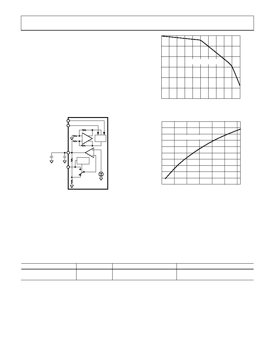
If the internal reference of the AD9649 is used to drive multiple
converters to improve gain matching, the loading of the reference
by the other converters must be considered. Figure 44 shows
how the internal reference voltage is affected by loading.
External Reference Operation
The use of an external reference may be necessary to enhance
the gain accuracy of the ADC or improve thermal drift charac-
teristics. Figure 45 shows the typical drift characteristics of the
internal reference in 1.0 V mode.
0
–3.0
02
LOAD CURRENT (mA)
RE
F
E
RE
NCE
V
O
L
T
AG
E
RR
O
R
(
%
)
.0
–0.5
–1.0
–1.5
–2.0
–2.5
0.2
0.4
0.6
0.8
1.0
1.4
1.6
1.8
1.2
INTERNAL VREF = 0.996V
08
53
9-
0
14
Figure 44. VREF Accuracy vs. Load Current
4
3
2
1
0
–1
–2
–3
–4
–5
–6
–40
–20
0
20
40
60
80
TEMPERATURE (°C)
V
RE
F
E
RRO
R
(
m
V
)
VREF ERROR (mV)
0
85
39
-05
2
Figure 45. Typical VREF Drift
When the SENSE pin is tied to AVDD, the internal reference is
disabled, allowing the use of an external reference. An internal
reference buffer loads the external reference with an equivalent
7.5 kΩ load (see Figure 28). The internal buffer generates the
positive and negative full-scale references for the ADC core.
Therefore, the external reference must be limited to a maximum
of 1.0 V.
Table 10. Reference Configuration Summary
Selected Mode
SENSE Voltage (V)
Resulting VREF (V)
Resulting Differential Span (V p-p)
Fixed Internal Reference
AGND to 0.2
1.0 internal
2.0
Fixed External Reference
AVDD
1.0 applied to external VREF pin
2.0
相关PDF资料 |
PDF描述 |
|---|---|
| VI-BN2-MW-F2 | CONVERTER MOD DC/DC 15V 100W |
| MS27656E25F61PB | CONN RCPT 61POS WALL MNT W/PINS |
| MS3100A16S-1P | CONN RCPT 7POS WALL MNT W/PINS |
| VI-BN2-MW-F1 | CONVERTER MOD DC/DC 15V 100W |
| LTC2864CS-2#PBF | IC TRANSCEIVER RS485 14-SOIC |
相关代理商/技术参数 |
参数描述 |
|---|---|
| AD9649BCPZRL7-80 | 功能描述:IC ADC 14BIT 80MSPS 32LFCSP RoHS:是 类别:集成电路 (IC) >> 数据采集 - 模数转换器 系列:- 标准包装:1 系列:- 位数:14 采样率(每秒):83k 数据接口:串行,并联 转换器数目:1 功率耗散(最大):95mW 电压电源:双 ± 工作温度:0°C ~ 70°C 安装类型:通孔 封装/外壳:28-DIP(0.600",15.24mm) 供应商设备封装:28-PDIP 包装:管件 输入数目和类型:1 个单端,双极 |
| AD9649W | 功能描述:IC ADC 制造商:analog devices inc. 系列:* 零件状态:上次购买时间 标准包装:1 |
| AD9649XCPZ-80 | 功能描述:14 Bit Analog to Digital Converter 1 Input 1 Pipelined 32-LFCSP-WQ (5x5) 制造商:analog devices inc. 系列:- 包装:托盘 零件状态:上次购买时间 位数:14 采样率(每秒):80M 输入数:1 输入类型:差分 数据接口:并联 配置:S/H-ADC 无线电 - S/H:ADC:1:1 A/D 转换器数:1 架构:管线 参考类型:内部 电压 - 电源,模拟:1.7 V ~ 1.9 V 电压 - 电源,数字:1.7 V ~ 3.6 V 特性:- 工作温度:-40°C ~ 85°C 封装/外壳:32-VFQFN 裸露焊盘,CSP 供应商器件封装:32-LFCSP-WQ(5x5) 标准包装:1 |
| AD9650 | 制造商:AD 制造商全称:Analog Devices 功能描述:16-Bit, 25 MSPS/65 MSPS/80 MSPS/105 MSPS, 1.8 V Dual Analog-to-Digital Converter (ADC) |
| AD9650-105EBZ | 功能描述:数据转换 IC 开发工具 16Bit Hi SNR 105 Msps Dual ADC RoHS:否 制造商:Texas Instruments 产品:Demonstration Kits 类型:ADC 工具用于评估:ADS130E08 接口类型:SPI 工作电源电压:- 6 V to + 6 V |
发布紧急采购,3分钟左右您将得到回复。