- 您现在的位置:买卖IC网 > PDF目录10113 > AD9649BCPZRL7-65 (Analog Devices Inc)IC ADC 14BIT 65MSPS 32LFCSP PDF资料下载
参数资料
| 型号: | AD9649BCPZRL7-65 |
| 厂商: | Analog Devices Inc |
| 文件页数: | 14/32页 |
| 文件大小: | 0K |
| 描述: | IC ADC 14BIT 65MSPS 32LFCSP |
| 标准包装: | 1,500 |
| 位数: | 14 |
| 采样率(每秒): | 65M |
| 数据接口: | 串行,SPI? |
| 转换器数目: | 1 |
| 功率耗散(最大): | 87.5mW |
| 电压电源: | 模拟和数字 |
| 工作温度: | -40°C ~ 85°C |
| 安装类型: | 表面贴装 |
| 封装/外壳: | 32-VFQFN 裸露焊盘,CSP |
| 供应商设备封装: | 32-LFCSP-VQ |
| 包装: | 带卷 (TR) |
| 输入数目和类型: | 2 个单端,单极;1 个差分,单极 |
第1页第2页第3页第4页第5页第6页第7页第8页第9页第10页第11页第12页第13页当前第14页第15页第16页第17页第18页第19页第20页第21页第22页第23页第24页第25页第26页第27页第28页第29页第30页第31页第32页
AD9649
Rev. 0 | Page 21 of
32
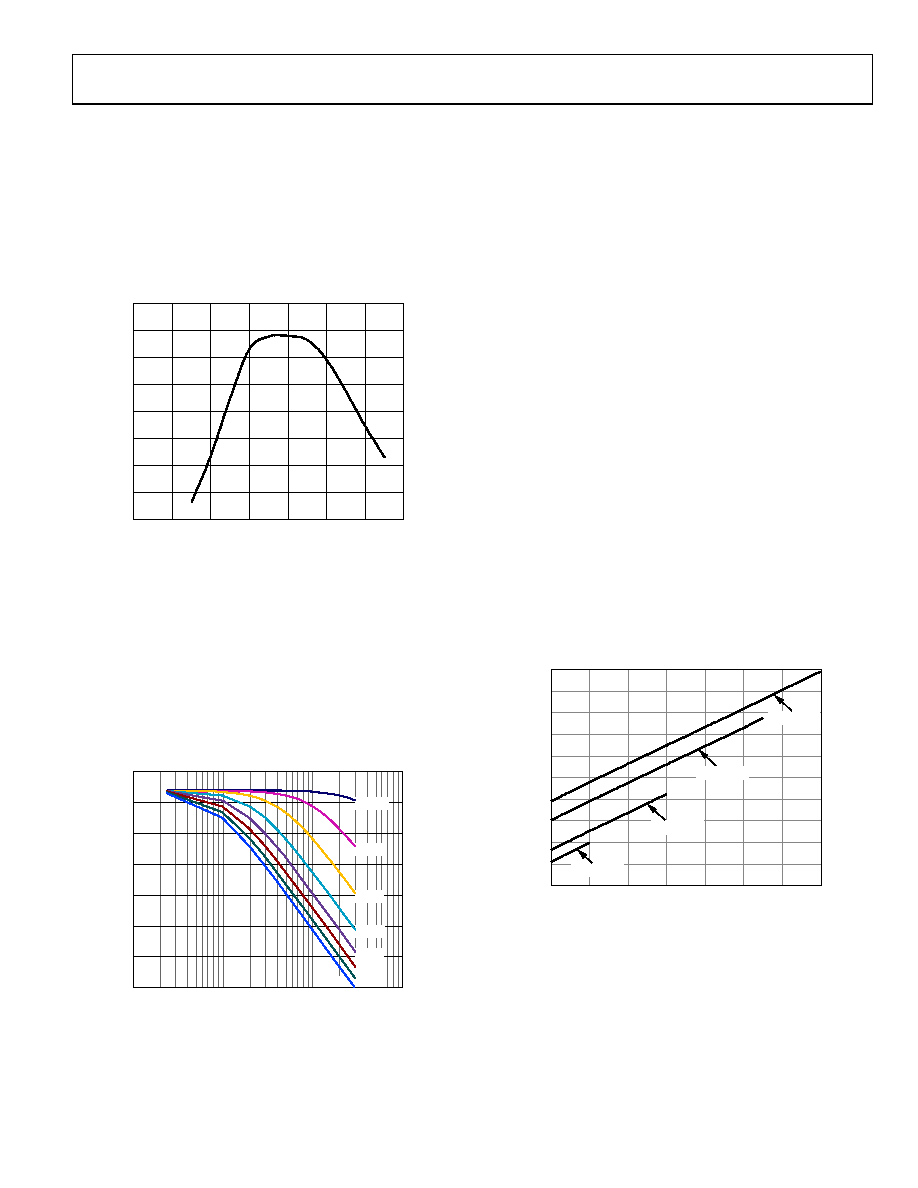
Clock Duty Cycle
Typical high speed ADCs use both clock edges to generate a
variety of internal timing signals and, as a result, may be sensitive
to clock duty cycle. Commonly, a 50% duty cycle clock with ±5%
tolerance is required to maintain optimum dynamic performance,
as shown in Figure 52.
Jitter on the rising edge of the clock input can also impact dynamic
performance and should be minimized, as discussed in the Jitter
Considerations section of this datasheet.
80
75
70
65
60
55
50
40
45
10
20
30
40
50
60
70
80
POSITIVE DUTY CYCLE (%)
S
N
R
(
d
BF
S
)
0
85
39
-0
53
Figure 52. SNR vs. Clock Duty Cycle
Jitter Considerations
High speed, high resolution ADCs are sensitive to the quality
of the clock input. The degradation in SNR from the low fre-
quency SNR (SNRLF) at a given input frequency (fINPUT) due to
jitter (tJRMS) can be calculated by
SNRHF = 10 log[(2π × fINPUT × tJRMS)2 + 10
]
)
10
/
(
LF
SNR
In the previous equation, the rms aperture jitter represents the
clock input jitter specification. IF undersampling applications
are particularly sensitive to jitter, as illustrated in Figure 53.
80
75
70
65
60
55
50
45
1
10
100
1k
FREQUENCY (MHz)
S
NR
(
d
BF
S
)
0.5ps
0.2ps
0.05ps
1.0ps
1.5ps
2.0ps
2.5ps
3.0ps
0
853
9-
0
22
Figure 53. SNR vs. Input Frequency and Jitter
The clock input should be treated as an analog signal in cases in
which aperture jitter may affect the dynamic range of the AD9649.
To avoid modulating the clock signal with digital noise, keep power
supplies for clock drivers separate from the ADC output driver
supplies. Low jitter, crystal-controlled oscillators make the best
clock sources. If the clock is generated from another type of source
(by gating, dividing, or another method), it should be retimed by
the original clock at the last step.
For more information, see the AN-501 Application Note and the
AN-756 Application Note, which are available on www.analog.com.
POWER DISSIPATION AND STANDBY MODE
As shown in Figure 54, the analog core power dissipated by the
AD9649 is proportional to its sample rate. The digital power dis-
sipation of the CMOS outputs are determined primarily by the
strength of the digital drivers and the load on each output bit.
The maximum DRVDD current (IDRVDD) can be calculated as
IDRVDD = VDRVDD × CLOAD × fCLK × N
where N is the number of output bits (15, in the case of the
AD9649).
This maximum current occurs when every output bit switches
on every clock cycle, that is, a full-scale square wave at the Nyquist
frequency of fCLK/2. In practice, the DRVDD current is estab-
lished by the average number of output bits that are switching,
which is determined by the sample rate and the characteristics
of the analog input signal.
Reducing the capacitive load presented to the output drivers can
minimize digital power consumption. The data in Figure 54 was
taken using the same operating conditions as those used for the
Typical Performance Characteristics, with a 5 pF load on each
output driver.
85
75
65
55
80
70
60
50
45
35
40
10
20
30
40
50
60
70
80
CLOCK RATE (MSPS)
ANAL
O
G
C
O
RE
P
O
W
E
R
(
m
W
)
AD9649-80
AD9649-65
AD9649-40
AD9649-20
08
53
9-
05
1
Figure 54. Analog Core Power vs. Clock Rate
In SPI mode, the AD9649 can be placed in power-down mode
directly via the SPI port or by using the programmable external
MODE pin. In non-SPI mode, power-down is achieved by assert-
ing the PDWN pin high. In this state, the ADC typically dissipates
500 μW. During power-down, the output drivers are placed in a
high impedance state. Asserting the PDWN pin (or the MODE pin
in SPI mode) low returns the AD9649 to normal operating mode.
Note that PDWN is referenced to the digital output driver supply
(DRVDD) and should not exceed that supply voltage.
相关PDF资料 |
PDF描述 |
|---|---|
| VI-BN2-MW-F2 | CONVERTER MOD DC/DC 15V 100W |
| MS27656E25F61PB | CONN RCPT 61POS WALL MNT W/PINS |
| MS3100A16S-1P | CONN RCPT 7POS WALL MNT W/PINS |
| VI-BN2-MW-F1 | CONVERTER MOD DC/DC 15V 100W |
| LTC2864CS-2#PBF | IC TRANSCEIVER RS485 14-SOIC |
相关代理商/技术参数 |
参数描述 |
|---|---|
| AD9649BCPZRL7-80 | 功能描述:IC ADC 14BIT 80MSPS 32LFCSP RoHS:是 类别:集成电路 (IC) >> 数据采集 - 模数转换器 系列:- 标准包装:1 系列:- 位数:14 采样率(每秒):83k 数据接口:串行,并联 转换器数目:1 功率耗散(最大):95mW 电压电源:双 ± 工作温度:0°C ~ 70°C 安装类型:通孔 封装/外壳:28-DIP(0.600",15.24mm) 供应商设备封装:28-PDIP 包装:管件 输入数目和类型:1 个单端,双极 |
| AD9649W | 功能描述:IC ADC 制造商:analog devices inc. 系列:* 零件状态:上次购买时间 标准包装:1 |
| AD9649XCPZ-80 | 功能描述:14 Bit Analog to Digital Converter 1 Input 1 Pipelined 32-LFCSP-WQ (5x5) 制造商:analog devices inc. 系列:- 包装:托盘 零件状态:上次购买时间 位数:14 采样率(每秒):80M 输入数:1 输入类型:差分 数据接口:并联 配置:S/H-ADC 无线电 - S/H:ADC:1:1 A/D 转换器数:1 架构:管线 参考类型:内部 电压 - 电源,模拟:1.7 V ~ 1.9 V 电压 - 电源,数字:1.7 V ~ 3.6 V 特性:- 工作温度:-40°C ~ 85°C 封装/外壳:32-VFQFN 裸露焊盘,CSP 供应商器件封装:32-LFCSP-WQ(5x5) 标准包装:1 |
| AD9650 | 制造商:AD 制造商全称:Analog Devices 功能描述:16-Bit, 25 MSPS/65 MSPS/80 MSPS/105 MSPS, 1.8 V Dual Analog-to-Digital Converter (ADC) |
| AD9650-105EBZ | 功能描述:数据转换 IC 开发工具 16Bit Hi SNR 105 Msps Dual ADC RoHS:否 制造商:Texas Instruments 产品:Demonstration Kits 类型:ADC 工具用于评估:ADS130E08 接口类型:SPI 工作电源电压:- 6 V to + 6 V |
发布紧急采购,3分钟左右您将得到回复。