参数资料
| 型号: | AD9709ASTZ |
| 厂商: | Analog Devices Inc |
| 文件页数: | 5/32页 |
| 文件大小: | 0K |
| 描述: | IC DAC 8BIT DUAL 125MSPS 48-LQFP |
| 产品培训模块: | Data Converter Fundamentals DAC Architectures |
| 标准包装: | 1 |
| 系列: | TxDAC+® |
| 设置时间: | 35ns |
| 位数: | 8 |
| 数据接口: | 并联 |
| 转换器数目: | 2 |
| 电压电源: | 模拟和数字 |
| 功率耗散(最大): | 450mW |
| 工作温度: | -40°C ~ 85°C |
| 安装类型: | 表面贴装 |
| 封装/外壳: | 48-LQFP |
| 供应商设备封装: | 48-LQFP(7x7) |
| 包装: | 托盘 |
| 输出数目和类型: | 4 电流,单极;4 电流,双极 |
| 采样率(每秒): | 125M |
| 产品目录页面: | 785 (CN2011-ZH PDF) |
| 配用: | AD9709-EBZ-ND - BOARD EVAL FOR AD9709 |
第1页第2页第3页第4页当前第5页第6页第7页第8页第9页第10页第11页第12页第13页第14页第15页第16页第17页第18页第19页第20页第21页第22页第23页第24页第25页第26页第27页第28页第29页第30页第31页第32页
AD9709
Rev. B | Page 13 of 32
The full-scale output current of each DAC is regulated by
separate reference control amplifiers and can be set from 2 mA
to 20 mA via an external network connected to the full-scale
adjust (FSADJ) pin. The external network in combination with
both the reference control amplifier and voltage reference
(VREFIO) sets the reference current (IREF), which is replicated to
the segmented current sources with the proper scaling factor.
The full-scale current (IOUTFS) is 32 × IREF.
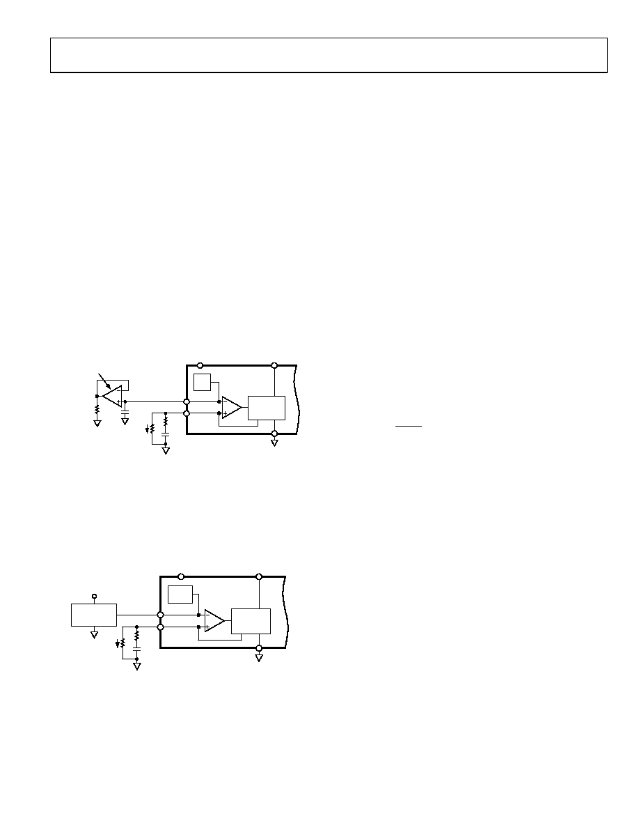
REFERENCE OPERATION
The AD9709 contains an internal 1.20 V band gap reference.
This can easily be overridden by a low noise external reference
with no effect on performance. REFIO serves as either an input
or output depending on whether the internal or an external
reference is used. To use the internal reference, simply decouple
the REFIO pin to ACOM with a 0.1 μF capacitor. The internal
reference voltage will be present at REFIO. If the voltage at
REFIO is to be used elsewhere in the circuit, an external buffer
amplifier with an input bias current of less than 100 nA should
be used. An example of the use of the internal reference is
shown in Figure 23.
AD9709
REFERENCE
SECTION
AVDD
GAINCTRL
REFIO
FSADJ1/
FSADJ2
ACOM
CURRENT
SOURCE
ARRAY
1.2V
REF
IREF
0.1F
OPTIONAL
EXTERNAL
REFERENCE
BUFFER
ADDITIONAL
EXTERNAL
LOAD
RSET
256
22nF
0060
6-
02
3
Figure 23. Internal Reference Configuration
An external reference can be applied to REFIO as shown in
Figure 24. The external reference can provide either a fixed
reference voltage to enhance accuracy and drift performance or
a varying reference voltage for gain control. Note that the 0.1 μF
compensation capacitor is not required because the internal
reference is overridden and the relatively high input impedance
of REFIO minimizes any loading of the external reference.
AD9709
REFERENCE
SECTION
AVDD
GAINCTRL
REFIO
FSADJ1/
FSADJ2
ACOM
AVDD
CURRENT
SOURCE
ARRAY
EXTERNAL
REFERENCE
1.2V
REF
0
06
-02
4
IREF
RSET
256
22nF
Figure 24. External Reference Configuration
GAIN CONTROL MODE
The AD9709 allows the gain of each channel to be set
independently by connecting one RSET resistor to FSADJ1 and
another RSET resistor to FSADJ2. To add flexibility and reduce
system cost, a single RSET resistor can be used to set the gain of
both channels simultaneously.
When GAINCTRL is low (that is, connected to analog ground),
the independent channel gain control mode using two resistors
is enabled. In this mode, individual RSET resistors should be
connected to FSADJ1 and FSADJ2. When GAINCTRL is high
(that is, connected to AVDD), the master/slave channel gain
control mode using one network is enabled. In this mode, a
single network is connected to FSADJ1, and the FSADJ2 pin
must be left unconnected.
Note that only parts with a date code of 9930 or later have the
master/slave gain control function. For parts with a date code
before 9930, Pin 42 must be connected to AGND, and the part
operates in the two-resistor, independent gain control mode.
SETTING THE FULL-SCALE CURRENT
Both of the DACs in the AD9709 contain a control amplifier
that is used to regulate the full-scale output current (IOUTFS). The
control amplifier is configured as a V-I converter, as shown in
of the VREFIO and an external resistor, RSET.
SET
REFIO
REF
R
V
I
=
The DAC full-scale current, IOUTFS, is an output current 32 times
larger than the reference current, IREF.
REF
OUTFS
I
×
= 32
The control amplifier allows a wide (10:1) adjustment span of
IOUTFS from 2 mA to 20 mA by setting IREF between 62.5 μA and
625 μA. The wide adjustment range of IOUTFS provides several
benefits. The first relates directly to the power dissipation of
Dissipation section). The second relates to the 20 dB adjustment,
which is useful for system gain control purposes.
It should be noted that when the RSET resistors are 2 kΩ or less,
the 22 nF capacitor and 256 Ω resistor shown in Figure 23 and
Figure 24 are not required and the reference current can be set
by the RSET resistors alone. For RSET values greater than 2 kΩ, the
22 nF capacitor and 256 Ω resistor networks are required to
ensure the stability of the reference control amplifier(s).
Regardless of the value of RSET, however, if the RSET resistor is
located more than ~10 cm away from the pin, use of the 22 nF
capacitor and 256 Ω resistor is recommended.
相关PDF资料 |
PDF描述 |
|---|---|
| MS27467T25F19PD | CONN PLUG 19POS STRAIGHT W/PINS |
| MS27466T25B29SB | CONN RCPT 29POS WALL MT W/SCKT |
| AD7392ARZ | IC DAC 12BIT PARALLEL 3V 20-SOIC |
| VE-J03-MZ-F4 | CONVERTER MOD DC/DC 24V 25W |
| VE-J03-MZ-F3 | CONVERTER MOD DC/DC 24V 25W |
相关代理商/技术参数 |
参数描述 |
|---|---|
| AD9709ASTZ1 | 制造商:AD 制造商全称:Analog Devices 功能描述:8-Bit, 125 MSPS, Dual TxDAC Digital-to-Analog Converter |
| AD9709ASTZKL1 | 制造商:Rochester Electronics LLC 功能描述: 制造商:Analog Devices 功能描述: |
| AD9709ASTZRL | 功能描述:IC DAC 8BIT DUAL 125MSPS 48LQFP RoHS:是 类别:集成电路 (IC) >> 数据采集 - 数模转换器 系列:TxDAC+® 产品培训模块:LTC263x 12-, 10-, and 8-Bit VOUT DAC Family 特色产品:LTC2636 - Octal 12-/10-/8-Bit SPI VOUT DACs with 10ppm/°C Reference 标准包装:91 系列:- 设置时间:4µs 位数:10 数据接口:MICROWIRE?,串行,SPI? 转换器数目:8 电压电源:单电源 功率耗散(最大):2.7mW 工作温度:-40°C ~ 85°C 安装类型:表面贴装 封装/外壳:14-WFDFN 裸露焊盘 供应商设备封装:14-DFN-EP(4x3) 包装:管件 输出数目和类型:8 电压,单极 采样率(每秒):* |
| AD9709ASTZRL1 | 制造商:AD 制造商全称:Analog Devices 功能描述:8-Bit, 125 MSPS, Dual TxDAC Digital-to-Analog Converter |
| AD9709-EB | 制造商:Analog Devices 功能描述: 制造商:Rochester Electronics LLC 功能描述: |
发布紧急采购,3分钟左右您将得到回复。