参数资料
| 型号: | AD9709ASTZ |
| 厂商: | Analog Devices Inc |
| 文件页数: | 7/32页 |
| 文件大小: | 0K |
| 描述: | IC DAC 8BIT DUAL 125MSPS 48-LQFP |
| 产品培训模块: | Data Converter Fundamentals DAC Architectures |
| 标准包装: | 1 |
| 系列: | TxDAC+® |
| 设置时间: | 35ns |
| 位数: | 8 |
| 数据接口: | 并联 |
| 转换器数目: | 2 |
| 电压电源: | 模拟和数字 |
| 功率耗散(最大): | 450mW |
| 工作温度: | -40°C ~ 85°C |
| 安装类型: | 表面贴装 |
| 封装/外壳: | 48-LQFP |
| 供应商设备封装: | 48-LQFP(7x7) |
| 包装: | 托盘 |
| 输出数目和类型: | 4 电流,单极;4 电流,双极 |
| 采样率(每秒): | 125M |
| 产品目录页面: | 785 (CN2011-ZH PDF) |
| 配用: | AD9709-EBZ-ND - BOARD EVAL FOR AD9709 |
第1页第2页第3页第4页第5页第6页当前第7页第8页第9页第10页第11页第12页第13页第14页第15页第16页第17页第18页第19页第20页第21页第22页第23页第24页第25页第26页第27页第28页第29页第30页第31页第32页
AD9709
Rev. B | Page 15 of 32
DIGITAL INPUTS
The digital inputs of the AD9709 consist of two independent
channels. For the dual port mode, each DAC has its own
dedicated 8-bit data port: WRT line and CLK line. In the
interleaved timing mode, the function of the digital control pins
changes as described in the Interleaved Mode Timing section.
The 8-bit parallel data inputs follow straight binary coding
where DB7P1 and DB7P2 are the most significant bits (MSBs)
and DB0P1 and DB0P2 are the least significant bits (LSBs).
IOUTA produces a full-scale output current when all data bits are
at Logic 1. IOUTB produces a complementary output with the
full-scale current split between the two outputs as a function of
the input code.
The digital interface is implemented using an edge-triggered
master slave latch. The DAC outputs are updated following
either the rising edge or every other rising edge of the clock,
depending on whether dual or interleaved mode is used. The
DAC outputs are designed to support a clock rate as high as
125 MSPS. The clock can be operated at any duty cycle that
meets the specified latch pulse width. The setup and hold times
can also be varied within the clock cycle as long as the specified
minimum times are met, although the location of these transition
edges may affect digital feedthrough and distortion performance.
Best performance is typically achieved when the input data
transitions on the falling edge of a 50% duty cycle clock.
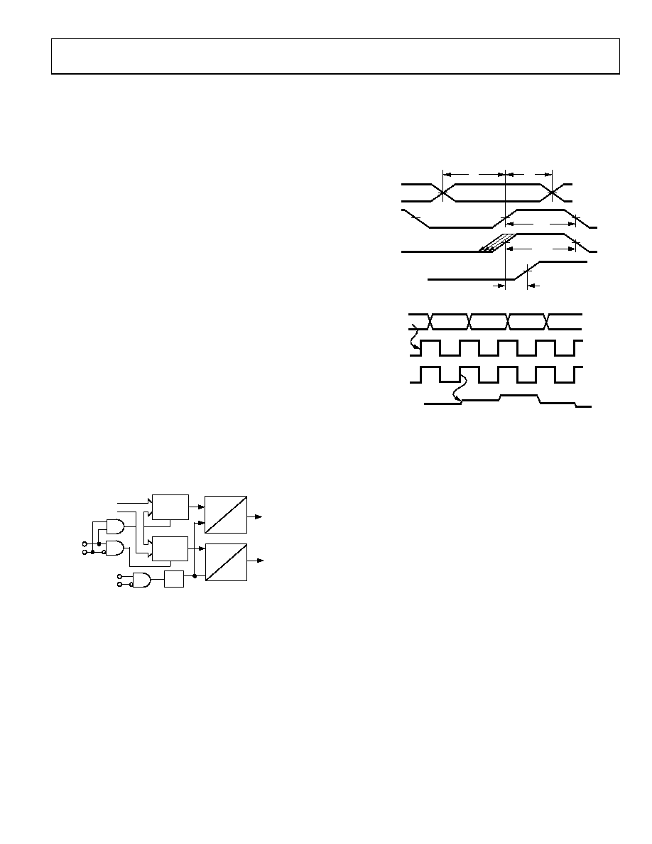
DAC TIMING
The AD9709 can operate in two timing modes, dual and
interleaved, which are described in the following sections. The
block diagram in Figure 25 represents the latch architecture in
the interleaved timing mode.
IQSEL
IQWRT
DAC1
INTERLEAVED
DATA IN, PORT 1
IQCLK
IQRESET
DAC2
÷2
PORT 1
INPUT
LATCH
PORT 2
INPUT
LATCH
DEINTERLEAVED
DATA OUT
DAC1
LATCH
DAC2
LATCH
00
60
6-
0
27
Figure 25. Latch Structure in Interleaved Mode
Dual Port Mode Timing
When the MODE pin is at Logic 1, the AD9709 operates in dual
port mode (refer to Figure 21). The AD9709 functions as two
distinct DACs. Each DAC has its own completely independent
digital input and control lines.
The AD9709 features a double-buffered data path. Data enters the
device through the channel input latches. This data is then trans-
ferred to the DAC latch in each signal path. After the data is loaded
into the DAC latch, the analog output settles to its new value.
For general consideration, the WRT lines control the channel
input latches, and the CLK lines control the DAC latches. Both
sets of latches are updated on the rising edge of their respective
control signals.
The rising edge of CLK should occur before or simultaneously
with the rising edge of WRT. If the rising edge of CLK occurs
after the rising edge of WRT, a minimum delay of 2 ns should
be maintained from rising edge of WRT to rising edge of CLK.
Timing specifications for dual port mode are given in Figure 26
and Figure 27.
DATA IN
WRT1/WRT2
CLK1/CLK2
tPD
IOUTA
OR
IOUTB
tS
tH
tLPW
tCPW
00
60
6-
0
25
Figure 26. Dual Port Mode Timing
DATA IN
WRT1/WRT2
CLK1/CLK2
XX
D1
D2
D3
D4
IOUTA
OR
IOUTB
D1
D2
D3
D4
D5
00
60
6-
02
6
Figure 27. Dual Mode Timing
Interleaved Mode Timing
When the MODE pin is at Logic 0, the AD9709 operates in
interleaved mode (refer to Figure 25). In addition, WRT1
functions as IQWRT, CLK1 functions as IQCLK, WRT2
functions as IQSEL, and CLK2 functions as IQRESET.
Data enters the device on the rising edge of IQWRT. The
logic level of IQSEL steers the data to either Channel Latch 1
(IQSEL = 1) or to Channel Latch 2 (IQSEL = 0). For proper
operation, IQSEL should only change state when IQWRT and
IQCLK are low.
When IQRESET is high, IQCLK is disabled. When IQRESET
goes low, the next rising edge on IQCLK updates both DAC
latches with the data present at their inputs. In the interleaved
mode, IQCLK is divided by 2 internally. Following this first
rising edge, the DAC latches are only updated on every other
rising edge of IQCLK. In this way, IQRESET can be used to
synchronize the routing of the data to the DACs.
Similar to the order of CLK and WRT in dual port mode,
IQCLK should occur before or simultaneously with IQWRT.
相关PDF资料 |
PDF描述 |
|---|---|
| MS27467T25F19PD | CONN PLUG 19POS STRAIGHT W/PINS |
| MS27466T25B29SB | CONN RCPT 29POS WALL MT W/SCKT |
| AD7392ARZ | IC DAC 12BIT PARALLEL 3V 20-SOIC |
| VE-J03-MZ-F4 | CONVERTER MOD DC/DC 24V 25W |
| VE-J03-MZ-F3 | CONVERTER MOD DC/DC 24V 25W |
相关代理商/技术参数 |
参数描述 |
|---|---|
| AD9709ASTZ1 | 制造商:AD 制造商全称:Analog Devices 功能描述:8-Bit, 125 MSPS, Dual TxDAC Digital-to-Analog Converter |
| AD9709ASTZKL1 | 制造商:Rochester Electronics LLC 功能描述: 制造商:Analog Devices 功能描述: |
| AD9709ASTZRL | 功能描述:IC DAC 8BIT DUAL 125MSPS 48LQFP RoHS:是 类别:集成电路 (IC) >> 数据采集 - 数模转换器 系列:TxDAC+® 产品培训模块:LTC263x 12-, 10-, and 8-Bit VOUT DAC Family 特色产品:LTC2636 - Octal 12-/10-/8-Bit SPI VOUT DACs with 10ppm/°C Reference 标准包装:91 系列:- 设置时间:4µs 位数:10 数据接口:MICROWIRE?,串行,SPI? 转换器数目:8 电压电源:单电源 功率耗散(最大):2.7mW 工作温度:-40°C ~ 85°C 安装类型:表面贴装 封装/外壳:14-WFDFN 裸露焊盘 供应商设备封装:14-DFN-EP(4x3) 包装:管件 输出数目和类型:8 电压,单极 采样率(每秒):* |
| AD9709ASTZRL1 | 制造商:AD 制造商全称:Analog Devices 功能描述:8-Bit, 125 MSPS, Dual TxDAC Digital-to-Analog Converter |
| AD9709-EB | 制造商:Analog Devices 功能描述: 制造商:Rochester Electronics LLC 功能描述: |
发布紧急采购,3分钟左右您将得到回复。