- 您现在的位置:买卖IC网 > PDF目录17064 > AD9726-EBZ (Analog Devices Inc)BOARD EVAL FOR AD9726 PDF资料下载
参数资料
| 型号: | AD9726-EBZ |
| 厂商: | Analog Devices Inc |
| 文件页数: | 11/24页 |
| 文件大小: | 0K |
| 描述: | BOARD EVAL FOR AD9726 |
| 产品培训模块: | DAC Architectures |
| 设计资源: | AD9726 Eval Brd Schematic AD9726 Eval Brd BOM |
| 标准包装: | 1 |
| 系列: | TxDAC+® |
| DAC 的数量: | 1 |
| 位数: | 16 |
| 采样率(每秒): | 400M |
| 数据接口: | 并联 |
| DAC 型: | 电流 |
| 工作温度: | -40°C ~ 85°C |
| 已供物品: | 板 |
| 已用 IC / 零件: | AD9726 |
| 相关产品: | AD9726BSVZ-ND - IC DAC 16IT LVDS 400MSPS 80-TQFP AD9726BSVZRL-ND - IC DAC 16IT LVDS 400MSPS 80-TQFP |
AD9726
Rev. B | Page 19 of 24
INTERNAL REFERENCE AND FULL-SCALE OUTPUT
The AD9726 contains an internal 1.2 V precision reference
source; this reference voltage appears at the REFIO pin. It can
be used to drive external circuitry if properly buffered.
Apply an external reference voltage source to the REFIO pin if
desired. The internal source is designed to be easily overdriven
by an external source; however, the internal reference can also
be powered down using the EXTREF bit in SPI Register 0x00.
The reference voltage (either internal or external) is applied to
an external precision resistor at the FSADJ pin. The resulting
current is internally amplified to provide the full-scale current
at the DAC output according to the following equation:
IOUTFS = VREF/RFSADJ × 32
Taking into account the binary value appearing at the data bus
inputs, the output currents IOUTA and IOUTB can be determined
according to the following equations:
IOUTA = IOUTFS × DB[15:0]/65536
IOUTB = IOUTFS × (1 DB[15:0])/65536
Note that the AD9726 features nonvolatile, factory-calibrated
gain using the internal reference source and a precision 2 kΩ
load. Gain accuracy in any application is, therefore, dependent
upon the accuracy of RFSADJ.
RESET
Following initial power-up and application of a valid DAC clock
signal, the AD9726 should always be initialized with an active
high pulse on the RESET pin. This defaults the programmable
registers, initializes volatile calibration memory, and prepares
the synchronization logic for data. The data bus should be static
prior to the reset pulse. After reset, LVDS data can flow.
The default state of the AD9726 is DDR and twos complement
binary input data. To use the AD9726 in this mode, it is not
necessary to program any device registers. However, the SPI is
enabled by default unless the SPI_DIS pin is connected high. If
not disabled, SPI input pins should not be left floating.
SERIAL PORT INTERFACE
The serial port interface is a flexible and synchronous serial
communications port allowing easy interface to many industry
standard microcontroller and microprocessor protocols
(including both Motorola SPI and Intel SSR). The interface
provides read/write access to registers that configure the
operation of the AD9726.
The AD9726 SPI supports single-byte and multibyte transfers as
well as MSB- or LSB-justified data formats. The interface can be
configured in 3-wire mode (in which SDIO is bidirectional) or
the default 4-wire mode (in which SDIO and SDO function as
unidirectional data input and data output, respectively).
Communication Cycle
All communication cycles have two phases. The first phase is
concerned with writing an instruction byte into the SPI
controller and always coincides with the first eight rising edges
of SCLK. The instruction byte provides the controller with
information regarding the second phase of the cycle, namely the
data transfer phase. The instruction byte contains the number
of data bytes to be transferred (one to four), a register address,
and a bit initiating a read or write operation.
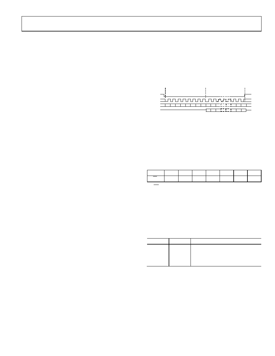
04540-010
CSB
INSTRUCTION CYCLE
DATA TRANSFER CYCLE
SCLK
SDIO
SDO
R/W
N1
N0
A4
A3
A2
A1
A0
D7n D6n
D20 D10 D00
Figure 23. SPI Communication Cycle
Any communication cycle begins with CSB going low, which
also resets the SPI control logic. Similarly, any communication
cycle ends with CSB going high, which aborts any incomplete
data transfer. After a communication cycle begins, the next
eight SCLK rising edges interpret data on the SDIO pin as the
instruction byte.
Instruction Byte
The instruction byte bits are shown in the following bit map.
B7
B6
B5
B4
B3
B2
B1
B0
R/W
N1
N0
A4
A3
A2
A1
A0
R/W
Bit 7 of the instruction byte selects a read or write transfer. If
the bit is set high, a read operation is indicated. If the bit is low,
a write operation is indicated.
N1, N0
Bit 6 and Bit 5 of the instruction byte determine the number of
data bytes to be transferred, as shown in Table 10.
Table 10.
N1
N0
Description
0
Transfer one data byte
0
1
Transfer two data bytes
1
0
Transfer three data bytes
1
Transfer four data bytes
A4, A3, A2, A1, A0
Bit 4 through Bit 0 of the instruction byte specify a 5-bit binary
value corresponding to a valid register address. In the case of
multibyte transfers, the location specified is either an initial or
a concluding register address. The SPI controller increments
or decrements this value to generate successive address values
depending on whether LSB or MSB justification is active.
相关PDF资料 |
PDF描述 |
|---|---|
| 0210490202 | CABLE JUMPER 1.25MM .178M 14POS |
| 0210490201 | CABLE JUMPER 1.25MM .178M 14POS |
| AP2182MPG-13 | IC PWR SW USB 2CH 1.5A 8-MSOP |
| 0210391009 | CABLE JUMPER 1MM .030M 31POS |
| DC1337A | BOARD SAR ADC LTC2309 |
相关代理商/技术参数 |
参数描述 |
|---|---|
| AD972A | 制造商:Analog Devices 功能描述:- Bulk |
| AD9731 | 制造商:AD 制造商全称:Analog Devices 功能描述:10-Bit, 170 MSPS D/A Converter |
| AD9731/PCB | 制造商:Analog Devices 功能描述:EVAL BOARDS FOR 10 BIT 125MHZ DAC - Bulk |
| AD97310713F | 制造商:Analog Devices 功能描述:- Rail/Tube |
发布紧急采购,3分钟左右您将得到回复。