参数资料
| 型号: | AD9744ARZRL |
| 厂商: | Analog Devices Inc |
| 文件页数: | 5/32页 |
| 文件大小: | 0K |
| 描述: | IC DAC 14BIT 210MSPS 28-SOIC |
| 产品培训模块: | Data Converter Fundamentals DAC Architectures |
| 标准包装: | 1,000 |
| 系列: | TxDAC® |
| 设置时间: | 11ns |
| 位数: | 14 |
| 数据接口: | 并联 |
| 转换器数目: | 1 |
| 电压电源: | 模拟和数字 |
| 功率耗散(最大): | 145mW |
| 工作温度: | -40°C ~ 85°C |
| 安装类型: | 表面贴装 |
| 封装/外壳: | 28-SOIC(0.295",7.50mm 宽) |
| 供应商设备封装: | 28-SOIC W |
| 包装: | 带卷 (TR) |
| 输出数目和类型: | 2 电流,单极;2 电流,双极 |
| 采样率(每秒): | 210M |
| 配用: | AD9744ACP-PCBZ-ND - BOARD EVAL FOR AD9744ACP |
第1页第2页第3页第4页当前第5页第6页第7页第8页第9页第10页第11页第12页第13页第14页第15页第16页第17页第18页第19页第20页第21页第22页第23页第24页第25页第26页第27页第28页第29页第30页第31页第32页
Data Sheet
AD9744
Rev. C | Page 13 of 32
FUNCTIONAL DESCRIPTION
Figure 23 shows a simplified block diagram of the AD9744. The
AD9744 consists of a DAC, digital control logic, and full-scale
output current control. The DAC contains a PMOS current
source array capable of providing up to 20 mA of full-scale
current (IOUTFS). The array is divided into 31 equal currents that
make up the five most significant bits (MSBs). The next four
bits, or middle bits, consist of 15 equal current sources whose
value is 1/16th of an MSB current source. The remaining LSBs
are binary weighted fractions of the middle bits current sources.
Implementing the middle and lower bits with current sources,
instead of an R-2R ladder, enhances its dynamic performance
for multitone or low amplitude signals and helps maintain the
DAC’s high output impedance (that is, >100 k).
All of these current sources are switched to one or the other of
the two output nodes, that is, IOUTA or IOUTB, via PMOS
differential current switches. The switches are based on the
architecture that was pioneered in the AD9764 family, with
further refinements to reduce distortion contributed by the
switching transient. This switch architecture also reduces
various timing errors and provides matching complementary
drive signals to the inputs of the differential current switches.
The analog and digital sections of the AD9744 have separate
power supply inputs, that is, AVDD and DVDD, that can operate
independently over a 2.7 V to 3.6 V range. The digital section,
which is capable of operating at a rate of up to 210 MSPS,
consists of edge-triggered latches and segment decoding logic
circuitry. The analog section includes the PMOS current
sources, the associated differential switches, a 1.2 V band gap
voltage reference, and a reference control amplifier.
The DAC full-scale output current is regulated by the reference
control amplifier and can be set from 2 mA to 20 mA via an
external resistor, RSET, connected to the full-scale adjust
(FS ADJ) pin. The external resistor, in combination with both
the reference control amplifier and voltage reference VREFIO, sets
the reference current IREF, which is replicated to the segmented
current sources with the proper scaling factor. The full-scale
current, IOUTFS, is 32 times IREF.
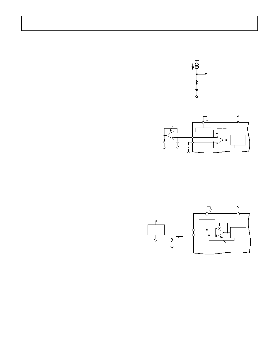
REFERENCE OPERATION
The AD9744 contains an internal 1.2 V band gap reference. The
internal reference cannot be disabled, but can be easily overridden
by an external reference with no effect on performance. Figure 25
shows an equivalent circuit of the band gap reference. REFIO
serves as either an output or an input depending on whether the
internal or an external reference is used. To use the internal
reference, simply decouple the REFIO pin to ACOM with a
0.1 F capacitor and connect REFLO to ACOM via a resistance
less than 5 . The internal reference voltage will be present at
REFIO. If the voltage at REFIO is to be used anywhere else in
the circuit, an external buffer amplifier with an input bias
current of less than 100 nA should be used. An example of the
use of the internal reference is shown in Figure 26.
Figure 25. Equivalent Circuit of Internal Reference
Figure 26. Internal Reference Configuration
An external reference can be applied to REFIO, as shown in
Figure 27. The external reference may provide either a fixed
reference voltage to enhance accuracy and drift performance or
a varying reference voltage for gain control. Note that the 0.1 F
compensation capacitor is not required since the internal reference
is overridden, and the relatively high input impedance of REFIO
minimizes any loading of the external reference.
Figure 27. External Reference Configuration
REFERENCE CONTROL AMPLIFIER
The AD9744 contains a control amplifier that is used to regulate
the full-scale output current, IOUTFS. The control amplifier is
configured as a V-I converter, as shown in Figure 26, so that its
current output, IREF, is determined by the ratio of the VREFIO and
an external resistor, RSET, as stated in Equation 4. IREF is copied
to the segmented current sources with the proper scale factor to
set IOUTFS, as stated in Equation 3.
AVDD
REFIO
REFLO
84
A
7k
02913-057
150pF
+1.2V REF
AVDD
REFLO
CURRENT
SOURCE
ARRAY
3.3V
REFIO
FS ADJ
2k
0.1
F
AD9744
ADDITIONAL
LOAD
OPTIONAL
EXTERNAL
REF BUFFER
02913-023
150pF
+1.2V REF
AVDD
REFLO
CURRENT
SOURCE
ARRAY
3.3V
REFIO
FS ADJ
RSET
AD9744
EXTERNAL
REF
IREF =
VREFIO/RSET
AVDD
REFERENCE
CONTROL
AMPLIFIER
VREFIO
02913-024
相关PDF资料 |
PDF描述 |
|---|---|
| V48A5H400BL3 | CONVERTER MOD DC/DC 5V 400W |
| V48A5H400BG | CONVERTER MOD DC/DC 5V 400W |
| V48A5H400B2 | CONVERTER MOD DC/DC 5V 400W |
| V48A3V3H264BL3 | CONVERTER MOD DC/DC 3.3V 264W |
| V48A3V3H264BG | CONVERTER MOD DC/DC 3.3V 264W |
相关代理商/技术参数 |
参数描述 |
|---|---|
| AD9744ARZRL1 | 制造商:AD 制造商全称:Analog Devices 功能描述:14-Bit, 210 MSPS TxDAC㈢ D/A Converter |
| AD9744-EB | 制造商:Analog Devices 功能描述:AD9744 EVALUATION BOARD (AD9744-EB) - Bulk |
| AD9745 | 制造商:AD 制造商全称:Analog Devices 功能描述:Dual 8-/10-/12-/14-/16-Bit 250 MSPS Digital-to-Analog Converters |
| AD9745BCPZ | 功能描述:IC DAC 2CH 12BIT 250MSPS 72LFCSP RoHS:是 类别:集成电路 (IC) >> 数据采集 - 数模转换器 系列:- 标准包装:1 系列:- 设置时间:4.5µs 位数:12 数据接口:串行,SPI? 转换器数目:1 电压电源:单电源 功率耗散(最大):- 工作温度:-40°C ~ 125°C 安装类型:表面贴装 封装/外壳:8-SOIC(0.154",3.90mm 宽) 供应商设备封装:8-SOICN 包装:剪切带 (CT) 输出数目和类型:1 电压,单极;1 电压,双极 采样率(每秒):* 其它名称:MCP4921T-E/SNCTMCP4921T-E/SNRCTMCP4921T-E/SNRCT-ND |
| AD9745BCPZRL | 功能描述:IC DAC DUAL 12B 250MSPS 72-LFCSP RoHS:是 类别:集成电路 (IC) >> 数据采集 - 数模转换器 系列:- 产品培训模块:Data Converter Fundamentals DAC Architectures 标准包装:750 系列:- 设置时间:7µs 位数:16 数据接口:并联 转换器数目:1 电压电源:双 ± 功率耗散(最大):100mW 工作温度:0°C ~ 70°C 安装类型:表面贴装 封装/外壳:28-LCC(J 形引线) 供应商设备封装:28-PLCC(11.51x11.51) 包装:带卷 (TR) 输出数目和类型:1 电压,单极;1 电压,双极 采样率(每秒):143k |
发布紧急采购,3分钟左右您将得到回复。