参数资料
| 型号: | AD9744ARZRL |
| 厂商: | Analog Devices Inc |
| 文件页数: | 9/32页 |
| 文件大小: | 0K |
| 描述: | IC DAC 14BIT 210MSPS 28-SOIC |
| 产品培训模块: | Data Converter Fundamentals DAC Architectures |
| 标准包装: | 1,000 |
| 系列: | TxDAC® |
| 设置时间: | 11ns |
| 位数: | 14 |
| 数据接口: | 并联 |
| 转换器数目: | 1 |
| 电压电源: | 模拟和数字 |
| 功率耗散(最大): | 145mW |
| 工作温度: | -40°C ~ 85°C |
| 安装类型: | 表面贴装 |
| 封装/外壳: | 28-SOIC(0.295",7.50mm 宽) |
| 供应商设备封装: | 28-SOIC W |
| 包装: | 带卷 (TR) |
| 输出数目和类型: | 2 电流,单极;2 电流,双极 |
| 采样率(每秒): | 210M |
| 配用: | AD9744ACP-PCBZ-ND - BOARD EVAL FOR AD9744ACP |
第1页第2页第3页第4页第5页第6页第7页第8页当前第9页第10页第11页第12页第13页第14页第15页第16页第17页第18页第19页第20页第21页第22页第23页第24页第25页第26页第27页第28页第29页第30页第31页第32页
Data Sheet
AD9744
Rev. C | Page 17 of 32
Figure 33. ICLKVDD vs. fCLOCK and Clock Mode
APPLYING THE AD9744
Output Configurations
The following sections illustrate some typical output configurations
for the AD9744. Unless otherwise noted, it is assumed that IOUTFS
is set to a nominal 20 mA. For applications requiring the optimum
dynamic performance, a differential output configuration is
suggested. A differential output configuration may consist of
either an RF transformer or a differential op amp configuration.
The transformer configuration provides the optimum high
frequency performance and is recommended for any application
that allows ac coupling. The differential op amp configuration is
suitable for applications requiring dc coupling, a bipolar output,
signal gain, and/or level shifting within the bandwidth of the
chosen op amp.
A single-ended output is suitable for applications requiring a
unipolar voltage output. A positive unipolar output voltage
results if IOUTA and/or IOUTB are connected to an appro-
priately sized load resistor, RLOAD, referred to ACOM. This
configuration may be more suitable for a single-supply system
requiring a dc-coupled, ground referred output voltage. Alter-
natively, an amplifier could be configured as an I-V converter,
thus converting IOUTA or IOUTB into a negative unipolar
voltage. This configuration provides the best dc linearity since
IOUTA or IOUTB is maintained at a virtual ground.
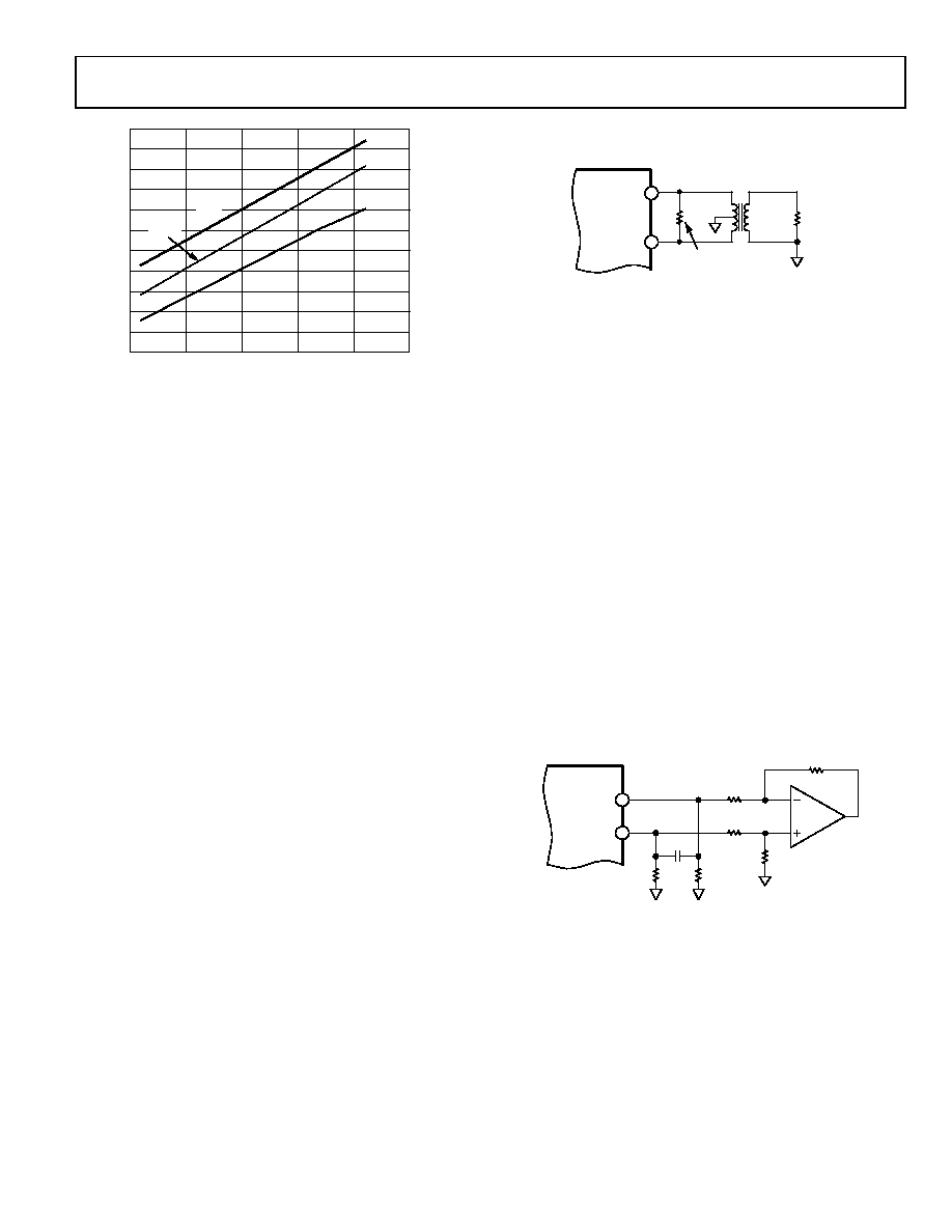
DIFFERENTIAL COUPLING USING A
TRANSFORMER
An RF transformer can be used to perform a differential-to-single-
ended signal conversion, as shown in Figure 34. A differentially
coupled transformer output provides the optimum distortion
performance for output signals whose spectral content lies
within the transformer’s pass band. An RF transformer, such as
the Mini-Circuits T1–1T, provides excellent rejection of
common-mode distortion (that is, even-order harmonics) and
noise over a wide frequency range. It also provides electrical
isolation and the ability to deliver twice the power to the load.
Transformers with different impedance ratios may also be used
for impedance matching purposes. Note that the transformer
provides ac coupling only.
Figure 34. Differential Output Using a Transformer
The center tap on the primary side of the transformer must be
connected to ACOM to provide the necessary dc current path
for both IOUTA and IOUTB. The complementary voltages
appearing at IOUTA and IOUTB (that is, VOUTA and VOUTB)
swing symmetrically around ACOM and should be maintained
with the specified output compliance range of the AD9744. A
differential resistor, RDIFF, may be inserted in applications where
the output of the transformer is connected to the load, RLOAD,
via a passive reconstruction filter or cable. RDIFF is determined
by the transformer’s impedance ratio and provides the proper
source termination that results in a low VSWR. Note that approx-
imately half the signal power will be dissipated across RDIFF.
DIFFERENTIAL COUPLING USING AN OP AMP
An op amp can also be used to perform a differential-to-single-
ended conversion, as shown in Figure 35. The AD9744 is
configured with two equal load resistors, RLOAD, of 25 Ω. The
differential voltage developed across IOUTA and IOUTB is
converted to a single-ended signal via the differential op amp
configuration. An optional capacitor can be installed across
IOUTA and IOUTB, forming a real pole in a low-pass filter. The
addition of this capacitor also enhances the op amp’s distortion
performance by preventing the DAC’s high slewing output from
overloading the op amp’s input.
Figure 35. DC Differential Coupling Using an Op Amp
The common-mode rejection of this configuration is typically
determined by the resistor matching. In this circuit, the differential
op amp circuit using the AD8047 is configured to provide some
additional signal gain. The op amp must operate off a dual supply
since its output is approximately ±1 V. A high speed amplifier
capable of preserving the differential performance of the AD9744
while meeting other system level objectives (such as cost or
power) should be selected. The op amp’s differential gain, gain
setting resistor values, and full-scale output swing capabilities
should all be considered when optimizing this circuit.
50
100
150
0
1
2
3
4
5
6
7
8
9
11
10
fCLOCK (MSPS)
I CLKV
DD
(mA)
250
200
0
SE
02913-030
PECL
DIFF
RLOAD
AD9744
MINI-CIRCUITS
T1-1T
OPTIONAL RDIFF
IOUTA
IOUTB
22
21
02913-031
AD9744
IOUTA
IOUTB
COPT
500
225
225
500
25
25
AD8047
02913-032
22
21
相关PDF资料 |
PDF描述 |
|---|---|
| V48A5H400BL3 | CONVERTER MOD DC/DC 5V 400W |
| V48A5H400BG | CONVERTER MOD DC/DC 5V 400W |
| V48A5H400B2 | CONVERTER MOD DC/DC 5V 400W |
| V48A3V3H264BL3 | CONVERTER MOD DC/DC 3.3V 264W |
| V48A3V3H264BG | CONVERTER MOD DC/DC 3.3V 264W |
相关代理商/技术参数 |
参数描述 |
|---|---|
| AD9744ARZRL1 | 制造商:AD 制造商全称:Analog Devices 功能描述:14-Bit, 210 MSPS TxDAC㈢ D/A Converter |
| AD9744-EB | 制造商:Analog Devices 功能描述:AD9744 EVALUATION BOARD (AD9744-EB) - Bulk |
| AD9745 | 制造商:AD 制造商全称:Analog Devices 功能描述:Dual 8-/10-/12-/14-/16-Bit 250 MSPS Digital-to-Analog Converters |
| AD9745BCPZ | 功能描述:IC DAC 2CH 12BIT 250MSPS 72LFCSP RoHS:是 类别:集成电路 (IC) >> 数据采集 - 数模转换器 系列:- 标准包装:1 系列:- 设置时间:4.5µs 位数:12 数据接口:串行,SPI? 转换器数目:1 电压电源:单电源 功率耗散(最大):- 工作温度:-40°C ~ 125°C 安装类型:表面贴装 封装/外壳:8-SOIC(0.154",3.90mm 宽) 供应商设备封装:8-SOICN 包装:剪切带 (CT) 输出数目和类型:1 电压,单极;1 电压,双极 采样率(每秒):* 其它名称:MCP4921T-E/SNCTMCP4921T-E/SNRCTMCP4921T-E/SNRCT-ND |
| AD9745BCPZRL | 功能描述:IC DAC DUAL 12B 250MSPS 72-LFCSP RoHS:是 类别:集成电路 (IC) >> 数据采集 - 数模转换器 系列:- 产品培训模块:Data Converter Fundamentals DAC Architectures 标准包装:750 系列:- 设置时间:7µs 位数:16 数据接口:并联 转换器数目:1 电压电源:双 ± 功率耗散(最大):100mW 工作温度:0°C ~ 70°C 安装类型:表面贴装 封装/外壳:28-LCC(J 形引线) 供应商设备封装:28-PLCC(11.51x11.51) 包装:带卷 (TR) 输出数目和类型:1 电压,单极;1 电压,双极 采样率(每秒):143k |
发布紧急采购,3分钟左右您将得到回复。