- 您现在的位置:买卖IC网 > PDF目录17063 > AD9748ACP-PCBZ (Analog Devices Inc)BOARD EVAL FOR AD9748ACP PDF资料下载
参数资料
| 型号: | AD9748ACP-PCBZ |
| 厂商: | Analog Devices Inc |
| 文件页数: | 9/24页 |
| 文件大小: | 0K |
| 描述: | BOARD EVAL FOR AD9748ACP |
| 产品培训模块: | DAC Architectures |
| 标准包装: | 1 |
| 系列: | TxDAC® |
| DAC 的数量: | 1 |
| 位数: | 8 |
| 采样率(每秒): | 210M |
| 数据接口: | 并联 |
| 设置时间: | 11ns |
| DAC 型: | 电流 |
| 工作温度: | -40°C ~ 85°C |
| 已供物品: | 板 |
| 已用 IC / 零件: | AD9748 |
| 相关产品: | AD9748ACPZ-ND - IC DAC 8BIT 210MSPS 32-LFCSP |
Data Sheet
AD9748
Rev. B | Page 17 of 24
POWER AND GROUNDING CONSIDERATIONS,
POWER SUPPLY REJECTION
Many applications seek high speed and high performance under
less than ideal operating conditions. In these application circuits,
the implementation and construction of the printed circuit
board is as important as the circuit design. Proper RF techniques
must be used for device selection, placement, and routing as
well as power supply bypassing and grounding to ensure
optimum performance. Figure 35 to Figure 38 illustrate the
recommended printed circuit board ground, power, and signal
plane layouts implemented on the AD9748 evaluation board.
One factor that can measurably affect system performance is
the ability of the DAC output to reject dc variations or ac noise
superimposed on the analog or digital dc power distribution.
This is referred to as the power supply rejection ratio (PSRR).
For dc variations of the power supply, the resulting performance
of the DAC directly corresponds to a gain error associated with
the DAC’s full-scale current, IOUTFS. AC noise on the dc supplies
is common in applications where the power distribution is
generated by a switching power supply. Typically, switching
power supply noise occurs over the spectrum from tens of
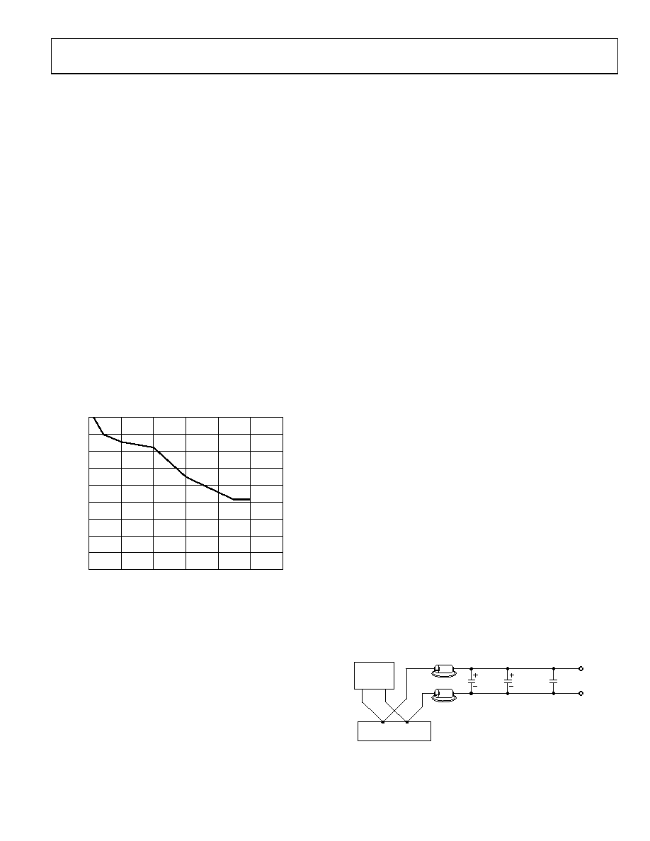
kilohertz to several megahertz. The PSRR vs. frequency of the
AD9748 AVDD supply over this frequency range is shown in
FREQUENCY (MHz)
85
40
12
6
8
10
0
PSRR
(dB)
80
75
70
65
60
55
50
2
4
45
03211-027
Figure 30. Power Supply Rejection Ratio (PSRR)
Note that the ratio in Figure 30 is calculated as amps out/volts
in. Noise on the analog power supply has the effect of modulating
the internal switches, and therefore the output current. The
voltage noise on AVDD, therefore, is added in a nonlinear
manner to the desired IOUT. Due to the relative different size of
these switches, the PSRR is very code dependent. This can produce
a mixing effect that can modulate low frequency power supply
noise to higher frequencies. Worst-case PSRR for either one of
the differential DAC outputs occurs when the full-scale current
is directed toward that output. As a result, the PSRR measurement
in Figure 30 represents a worst-case condition in which the
digital inputs remain static and the full-scale output current of
20 mA is directed to the DAC output being measured.
The following illustrates the effect of supply noise on the analog
supply. Suppose a switching regulator with a switching
frequency of 250 kHz produces 10 mV of noise and, for simplicity’s
sake (ignoring harmonics), all of this noise is concentrated at
250 kHz. To calculate how much of this undesired noise appears as
current noise superimposed on the DAC’s full-scale current,
250 kHz. To calculate the PSRR for a given RLOAD, such that the
units of PSRR are converted from A/V to V/V, adjust the curve
in Figure 30 by the scaling factor 20
log(R
LOAD
). For instance,
if RLOAD is 50 , then the PSRR is reduced by 34 dB (that is,
PSRR of the DAC at 250 kHz, which is 85 dB in Figure 30,
becomes 51 dB VOUT/VIN).
Proper grounding and decoupling should be a primary
objective in any high speed, high resolution system. The
AD9748 features separate analog and digital supplies and
ground pins to optimize the management of analog and digital
ground currents in a system. In general, AVDD, the analog
supply, should be decoupled to ACOM, the analog common,
as close to the chip as physically possible. Similarly, DVDD, the
digital supply, should be decoupled to DCOM as close to the
chip as physically possible.
For those applications that require a single 3.3 V supply for both
the analog and digital supplies, a clean analog supply can be
generated using the circuit shown in Figure 31. The circuit
consists of a differential LC filter with separate power supply
and return lines. Lower noise can be attained by using low ESR
type electrolytic and tantalum capacitors.
100
F
ELECT.
0.1
F
CER.
TTL/CMOS
LOGIC
CIRCUITS
3.3V
POWER SUPPLY
FERRITE
BEADS
AVDD
ACOM
10
F–22F
TANT.
03211-028
Figure 31. Differential LC Filter for Single 3.3 V Applications
相关PDF资料 |
PDF描述 |
|---|---|
| GCM18DCTD-S288 | CONN EDGECARD 36POS .156 EXTEND |
| GBM24DSEI-S243 | CONN EDGECARD 48POS .156 EYELET |
| GBM15DSEF-S243 | CONN EDGECARD 30POS .156 EYELET |
| GCM10DCST-S288 | CONN EDGECARD 20POS .156 EXTEND |
| SEK332M016ST | CAP ALUM 3300UF 16V 20% RADIAL |
相关代理商/技术参数 |
参数描述 |
|---|---|
| AD9748ACPRL7 | 制造商:Analog Devices 功能描述:DAC 1-CH Segment 8-bit 32-Pin LFCSP EP T/R |
| AD9748ACPZ | 功能描述:IC DAC 8BIT 210MSPS 32-LFCSP RoHS:是 类别:集成电路 (IC) >> 数据采集 - 数模转换器 系列:TxDAC® 产品培训模块:Lead (SnPb) Finish for COTS Obsolescence Mitigation Program 标准包装:50 系列:- 设置时间:4µs 位数:12 数据接口:串行 转换器数目:2 电压电源:单电源 功率耗散(最大):- 工作温度:-40°C ~ 85°C 安装类型:表面贴装 封装/外壳:8-TSSOP,8-MSOP(0.118",3.00mm 宽) 供应商设备封装:8-uMAX 包装:管件 输出数目和类型:2 电压,单极 采样率(每秒):* 产品目录页面:1398 (CN2011-ZH PDF) |
| AD9748ACPZ | 制造商:Analog Devices 功能描述:DAC, 8BIT, 210MSPS, LFCSP-32 |
| AD9748ACPZRL7 | 功能描述:IC DAC 8BIT 210MSPS 32LFCSP RoHS:是 类别:集成电路 (IC) >> 数据采集 - 数模转换器 系列:TxDAC® 产品培训模块:LTC263x 12-, 10-, and 8-Bit VOUT DAC Family 特色产品:LTC2636 - Octal 12-/10-/8-Bit SPI VOUT DACs with 10ppm/°C Reference 标准包装:91 系列:- 设置时间:4µs 位数:10 数据接口:MICROWIRE?,串行,SPI? 转换器数目:8 电压电源:单电源 功率耗散(最大):2.7mW 工作温度:-40°C ~ 85°C 安装类型:表面贴装 封装/外壳:14-WFDFN 裸露焊盘 供应商设备封装:14-DFN-EP(4x3) 包装:管件 输出数目和类型:8 电压,单极 采样率(每秒):* |
| AD9748XCP | 制造商:AD 制造商全称:Analog Devices 功能描述:8-Bit, 165 MSPS TxDAC D/A Converter |
发布紧急采购,3分钟左右您将得到回复。