- 您现在的位置:买卖IC网 > PDF目录17063 > AD9751-EB (Analog Devices Inc)BOARD EVAL FOR AD9751 PDF资料下载
参数资料
| 型号: | AD9751-EB |
| 厂商: | Analog Devices Inc |
| 文件页数: | 3/28页 |
| 文件大小: | 0K |
| 描述: | BOARD EVAL FOR AD9751 |
| 产品培训模块: | DAC Architectures |
| 标准包装: | 1 |
| 系列: | TxDAC® |
| DAC 的数量: | 1 |
| 位数: | 10 |
| 采样率(每秒): | 300M |
| 数据接口: | 并联 |
| 设置时间: | 11ns |
| DAC 型: | 电流 |
| 工作温度: | -40°C ~ 85°C |
| 已供物品: | 板 |
| 已用 IC / 零件: | AD9751 |
| 相关产品: | AD9751ASTZRL-ND - IC DAC 10BIT 300MSPS 48LQFP AD9751ASTZ-ND - IC DAC 10BIT 300MSPS 48-LQFP |
第1页第2页当前第3页第4页第5页第6页第7页第8页第9页第10页第11页第12页第13页第14页第15页第16页第17页第18页第19页第20页第21页第22页第23页第24页第25页第26页第27页第28页
REV. C
AD9751
–11–
1.2V REF
AVDD
IREF
CURRENT
SOURCE
ARRAY
REFIO
FSADJ
2k
0.1 F
AD9751
REFERENCE
SECTION
ADDITIONAL
EXTERNAL
LOAD
OPTIONAL
EXTERNAL
REFERENCE
BUFFER
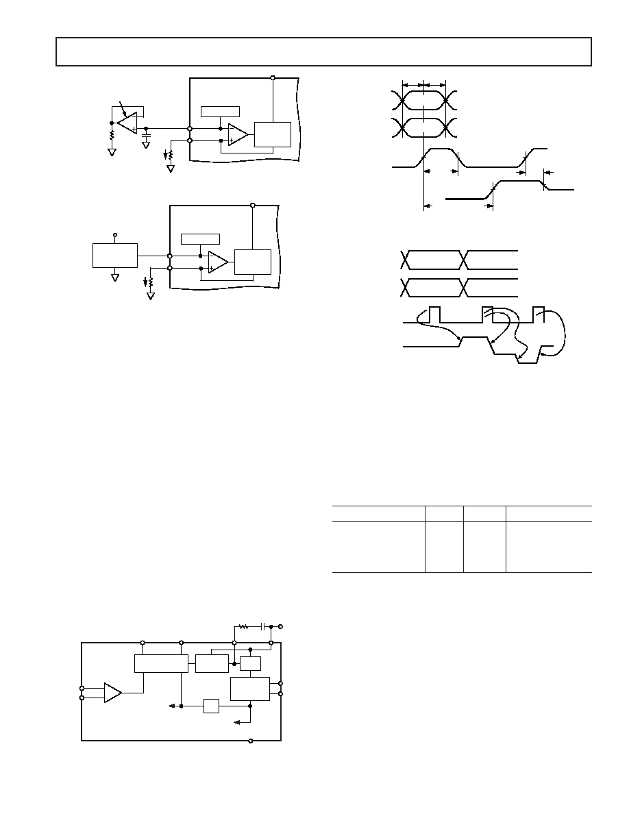
Figure 4. Internal Reference Configuration
1.2V REF
AVDD
IREF
CURRENT
SOURCE
ARRAY
REFIO
FSADJ
2k
AD9751
REFERENCE
SECTION
EXTERNAL
REFERENCE
AVDD
Figure 5. External Reference Configuration
PLL CLOCK MULTIPLIER OPERATION
The Phase-Locked Loop (PLL) is intrinsic to the operation of the
AD9751 in that it produces the necessary internally synchronized
2
× clock for the edge-triggered latches, multiplexer, and DAC.
With PLLVDD connected to its supply voltage, the AD9751 is
in PLL active mode. Figure 6 shows a functional block diagram
of the AD9751 clock control circuitry with PLL active. The
circuitry consists of a phase detector, charge pump, voltage
controlled oscillator (VCO), input data rate range control, clock
logic circuitry, and control input/outputs. The
÷2 logic in the
feedback loop allows the PLL to generate the 2
× clock needed
for the DAC output latch.
Figure 7 defines the input and output timing for the AD9751
with the PLL active. CLK in Figure 7 represents the clock that
is generated external to the AD9751. The input data at both
Ports 1 and 2 is latched on the same CLK rising edge. CLK
may be applied as a single-ended signal by tying CLK– to
midsupply and applying CLK to CLK+, or as a differential
signal applied to CLK+ and CLK–.
RESET has no purpose when using the internal PLL and
should be grounded. When the AD9751 is in PLL active
mode, PLLLOCK is the output of the internal phase detector.
When locked, the lock output in this mode is Logic 1.
CLKCOM
TO INPUT
LATCHES
CLKVDD
(3.0V TO 3.6V)
PLLLOCK
CHARGE
PUMP
PHASE
DETECTOR
LPF
PLLVDD
VCO
392
1.0 F
3.0V TO
3.6V
RANGE
CONTROL
(
1, 2, 4, 8)
DIV0
DIV1
DIFFERENTIAL
TO
SINGLE-ENDED
AMP
2
TO DAC
LATCH
CLK+
CLK–
AD9751
Figure 6. Clock Circuitry with PLL Active
PORT 1
DATA X
DATA Y
tH
tS
tLPW
tPD
DATA X
DATA Y
1/2 CYCLE +
tPD
PORT 2
IOUTA OR IOUTB
CLK
DATA IN
7a. DAC Input Timing Requirements with
PLL Active, Single Clock Cycle
PORT 1
DATA X
DATA Z
DATA X
DATA Y
PORT 2
IOUTA OR IOUTB
CLK
DATA IN
DATA Z
DATA W
XXX
DATA W
DATA Y
Figure 7b. DAC Input Timing Requirements with
PLL Active, Multiple Clock Cycles
Typically, the VCO can generate outputs of 100 MHz to 400 MHz.
The range control is used to keep the VCO operating within its
designed range while allowing input clocks as low as 6.25 MHz.
With the PLL active, logic levels at DIV0 and DIV1 determine
the divide (prescaler) ratio of the range controller. Table I gives
the frequency range of the input clock for the different states of
DIV0 and DIV1.
Table I. CLK Rates for DIV0, DIV1 Levels with PLL Active
CLK Frequency
DIV1
DIV0
Range Controller
50 MHz–150 MHz
0
÷1
25 MHz–100 MHz
0
1
÷2
12.5 MHz–50 MHz
1
0
÷4
6.25 MHz–25 MHz
1
÷8
A 392
resistor and 1.0 F capacitor connected in series from
LPF to PLLVDD are required to optimize the phase noise versus
settling/acquisition time characteristics of the PLL. To obtain
optimum noise and distortion performance, PLLVDD should
be set to a voltage level similar to DVDD and CLKVDD.
In general, the best phase noise performance for any PLL range
control setting is achieved with the VCO operating near its
maximum output frequency of 400 MHz.
As stated earlier, applications requiring input data rates below
6.25 MSPS must disable the PLL clock multiplier and provide an
external 2
× reference clock. At higher data rates however, applica-
tions already containing a low phase noise (i.e., jitter) reference
clock that is twice the input data rate should consider disabling the
PLL clock multiplier to achieve the best SNR performance from the
AD9751. Note that the SFDR performance of the AD9751 remains
unaffected with or without the PLL clock multiplier enabled.
相关PDF资料 |
PDF描述 |
|---|---|
| MLG1005S10NJ | INDUCTOR MULTILAYER 10NH 0402 |
| GCM10DCMT-S288 | CONN EDGECARD 20POS .156 EXTEND |
| UPB2E271MRD | CAP ALUM 270UF 250V 20% RADIAL |
| ECE-V1EA101P | CAP ALUM 100UF 25V 20% SMD |
| MLK1005S15NJ | INDUCTOR MULTILAYER 15NH 0402 |
相关代理商/技术参数 |
参数描述 |
|---|---|
| AD9752 | 制造商:AD 制造商全称:Analog Devices 功能描述:12-Bit, 125 MSPS High Performance TxDAC D/A Converter |
| AD9752AR | 功能描述:IC DAC 12BIT 125MSPS 28-SOIC RoHS:否 类别:集成电路 (IC) >> 数据采集 - 数模转换器 系列:TxDAC® 产品培训模块:Data Converter Fundamentals DAC Architectures 标准包装:750 系列:- 设置时间:7µs 位数:16 数据接口:并联 转换器数目:1 电压电源:双 ± 功率耗散(最大):100mW 工作温度:0°C ~ 70°C 安装类型:表面贴装 封装/外壳:28-LCC(J 形引线) 供应商设备封装:28-PLCC(11.51x11.51) 包装:带卷 (TR) 输出数目和类型:1 电压,单极;1 电压,双极 采样率(每秒):143k |
| AD9752ARRL | 制造商:Analog Devices 功能描述:DAC 1-CH Segment 12-bit 28-Pin SOIC W T/R 制造商:Rochester Electronics LLC 功能描述:12-BIT 125 MSPS+ TXDAC D/A CONVERTER - Tape and Reel |
| AD9752ARU | 功能描述:IC DAC 12BIT 125MSPS HP 28-TSSOP RoHS:否 类别:集成电路 (IC) >> 数据采集 - 数模转换器 系列:TxDAC® 产品培训模块:Data Converter Fundamentals DAC Architectures 标准包装:750 系列:- 设置时间:7µs 位数:16 数据接口:并联 转换器数目:1 电压电源:双 ± 功率耗散(最大):100mW 工作温度:0°C ~ 70°C 安装类型:表面贴装 封装/外壳:28-LCC(J 形引线) 供应商设备封装:28-PLCC(11.51x11.51) 包装:带卷 (TR) 输出数目和类型:1 电压,单极;1 电压,双极 采样率(每秒):143k |
发布紧急采购,3分钟左右您将得到回复。