- 您现在的位置:买卖IC网 > PDF目录17063 > AD9751-EB (Analog Devices Inc)BOARD EVAL FOR AD9751 PDF资料下载
参数资料
| 型号: | AD9751-EB |
| 厂商: | Analog Devices Inc |
| 文件页数: | 9/28页 |
| 文件大小: | 0K |
| 描述: | BOARD EVAL FOR AD9751 |
| 产品培训模块: | DAC Architectures |
| 标准包装: | 1 |
| 系列: | TxDAC® |
| DAC 的数量: | 1 |
| 位数: | 10 |
| 采样率(每秒): | 300M |
| 数据接口: | 并联 |
| 设置时间: | 11ns |
| DAC 型: | 电流 |
| 工作温度: | -40°C ~ 85°C |
| 已供物品: | 板 |
| 已用 IC / 零件: | AD9751 |
| 相关产品: | AD9751ASTZRL-ND - IC DAC 10BIT 300MSPS 48LQFP AD9751ASTZ-ND - IC DAC 10BIT 300MSPS 48-LQFP |
第1页第2页第3页第4页第5页第6页第7页第8页当前第9页第10页第11页第12页第13页第14页第15页第16页第17页第18页第19页第20页第21页第22页第23页第24页第25页第26页第27页第28页
REV. C
AD9751
–17–
The center tap on the primary side of the transformer must be
connected to ACOM to provide the necessary dc current path
for both IOUTA and IOUTB. The complementary voltages appearing
at IOUTA and IOUTB (i.e., VOUTA and VOUTB) swing symmetrically
around ACOM and should be maintained with the specified
output compliance range of the AD9751. A differential resistor,
RDIFF, may be inserted into applications where the output of the
transformer is connected to the load, RLOAD, via a passive recon-
struction filter or cable. RDIFF is determined by the transformer’s
impedance ratio and provides the proper source termination that
results in a low VSWR.
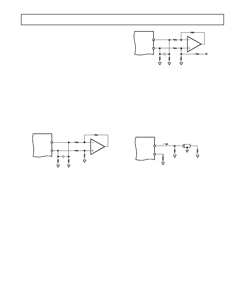
DIFFERENTIAL COUPLING USING AN OP AMP
An op amp can also be used to perform a differential-to-
single-ended conversion, as shown in Figure 21. The AD9751
is configured with two equal load resistors, RLOAD, of 25
. The
differential voltage developed across IOUTA and IOUTB is con-
verted to a single-ended signal via the differential op amp
configuration. An optional capacitor can be installed across
IOUTA and IOUTB, forming a real pole in a low-pass filter. The
addition of this capacitor also enhances the op amp’s distortion
performance by preventing the DAC’s high slewing output from
overloading the op amp’s input.
AD9751
IOUTA
IOUTB
COPT
500
225
500
25
AD8047
Figure 21. DC Differential Coupling Using an Op Amp
The common-mode rejection of this configuration is typically
determined by the resistor matching. In this circuit, the dif-
ferential op amp circuit using the AD8047 is configured to
provide some additional signal gain. The op amp must operate
from a dual supply since its output is approximately
± 1.0 V.
A high speed amplifier capable of preserving the differential
performance of the AD9751, while meeting other system-
level objectives (i.e., cost, power), should be selected. The op
amp’s differential gain, gain setting resistor values, and full-
scale output swing capabilities should all be considered when
optimizing this circuit.
The differential circuit shown in Figure 22 provides the nec-
essary level-shifting required in a single-supply system. In this
case, AVDD, which is the positive analog supply for both the
AD9751 and the op amp, is also used to level-shift the differ-
ential output of the AD9751 to midsupply (i.e., AVDD/2). The
AD8041 is a suitable op amp for this application.
AD9751
IOUTA
IOUTB
COPT
500
225
1k
25
AD8041
1k
AVDD
Figure 22. Single-Supply DC Differential Coupled Circuit
SINGLE-ENDED UNBUFFERED VOLTAGE OUTPUT
Figure 23 shows the AD9751 configured to provide a unipolar
output range of approximately 0 V to 0.5 V for a doubly-termi-
nated 50
cable, since the nominal full-scale current, I
OUTFS, of
20 mA flows through the equivalent RLOAD of 25
. In this case,
RLOAD represents the equivalent load resistance seen by IOUTA or
IOUTB. The unused output (IOUTA or IOUTB) can be connected to
ACOM directly or via a matching RLOAD. Different values of
IOUTFS and RLOAD can be selected as long as the positive com-
pliance range is adhered to. One additional consideration in
this mode is the integral nonlinearity (INL), as discussed in the
Analog Outputs section. For optimum INL performance, the
single-ended, buffered voltage output configuration is suggested.
AD9751
IOUTA
IOUTB
50
25
50
VOUTA = 0V TO 0.5V
IOUTFS = 20mA
Figure 23. 0 V to 0.5 V Unbuffered Voltage Output
SINGLE-ENDED BUFFERED VOLTAGE OUTPUT
Figure 24 shows a buffered single-ended output configuration in
which the op amp performs an I–V conversion on the AD9751
output current. The op amp maintains IOUTA (or IOUTB) at a
virtual ground, thus minimizing the nonlinear output impedance
effect on the DAC’s INL performance as discussed in the
Analog Output section. Although this single-ended configura-
tion typically provides the best dc linearity performance, its ac
distortion performance at higher DAC update rates may be
limited by the op amp’s slewing capabilities. The op amp pro-
vides a negative unipolar output voltage and its full-scale output
voltage is simply the product of RFB and IOUTFS. The full-scale
output should be set within the op amp’s voltage output swing
capabilities by scaling IOUTFS and/or RFB. An improvement in ac
distortion performance may result with a reduced IOUTFS, since
the signal current the op amp will be required to sink will subse-
quently be reduced.
相关PDF资料 |
PDF描述 |
|---|---|
| MLG1005S10NJ | INDUCTOR MULTILAYER 10NH 0402 |
| GCM10DCMT-S288 | CONN EDGECARD 20POS .156 EXTEND |
| UPB2E271MRD | CAP ALUM 270UF 250V 20% RADIAL |
| ECE-V1EA101P | CAP ALUM 100UF 25V 20% SMD |
| MLK1005S15NJ | INDUCTOR MULTILAYER 15NH 0402 |
相关代理商/技术参数 |
参数描述 |
|---|---|
| AD9752 | 制造商:AD 制造商全称:Analog Devices 功能描述:12-Bit, 125 MSPS High Performance TxDAC D/A Converter |
| AD9752AR | 功能描述:IC DAC 12BIT 125MSPS 28-SOIC RoHS:否 类别:集成电路 (IC) >> 数据采集 - 数模转换器 系列:TxDAC® 产品培训模块:Data Converter Fundamentals DAC Architectures 标准包装:750 系列:- 设置时间:7µs 位数:16 数据接口:并联 转换器数目:1 电压电源:双 ± 功率耗散(最大):100mW 工作温度:0°C ~ 70°C 安装类型:表面贴装 封装/外壳:28-LCC(J 形引线) 供应商设备封装:28-PLCC(11.51x11.51) 包装:带卷 (TR) 输出数目和类型:1 电压,单极;1 电压,双极 采样率(每秒):143k |
| AD9752ARRL | 制造商:Analog Devices 功能描述:DAC 1-CH Segment 12-bit 28-Pin SOIC W T/R 制造商:Rochester Electronics LLC 功能描述:12-BIT 125 MSPS+ TXDAC D/A CONVERTER - Tape and Reel |
| AD9752ARU | 功能描述:IC DAC 12BIT 125MSPS HP 28-TSSOP RoHS:否 类别:集成电路 (IC) >> 数据采集 - 数模转换器 系列:TxDAC® 产品培训模块:Data Converter Fundamentals DAC Architectures 标准包装:750 系列:- 设置时间:7µs 位数:16 数据接口:并联 转换器数目:1 电压电源:双 ± 功率耗散(最大):100mW 工作温度:0°C ~ 70°C 安装类型:表面贴装 封装/外壳:28-LCC(J 形引线) 供应商设备封装:28-PLCC(11.51x11.51) 包装:带卷 (TR) 输出数目和类型:1 电压,单极;1 电压,双极 采样率(每秒):143k |
发布紧急采购,3分钟左右您将得到回复。