参数资料
| 型号: | AD9754ARUZRL7 |
| 厂商: | Analog Devices Inc |
| 文件页数: | 24/24页 |
| 文件大小: | 0K |
| 描述: | IC DAC 14BIT 125MSPS 28-TSSOP |
| 产品培训模块: | Data Converter Fundamentals DAC Architectures |
| 标准包装: | 1,000 |
| 系列: | TxDAC® |
| 设置时间: | 35ns |
| 位数: | 14 |
| 数据接口: | 并联 |
| 转换器数目: | 1 |
| 电压电源: | 模拟和数字 |
| 功率耗散(最大): | 220mW |
| 工作温度: | -40°C ~ 85°C |
| 安装类型: | 表面贴装 |
| 封装/外壳: | 28-TSSOP(0.173",4.40mm 宽) |
| 供应商设备封装: | 28-TSSOP |
| 包装: | 带卷 (TR) |
| 输出数目和类型: | 1 电流,单极;1 电流,双极 |
| 采样率(每秒): | 125M |
| 其它名称: | AD9754ARUZRL7-ND AD9754ARUZRL7TR |
AD9754
–9–
REV. A
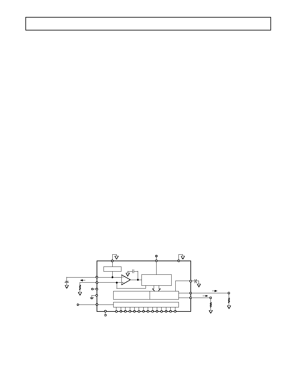
FUNCTIONAL DESCRIPTION
Figure 16 shows a simplified block diagram of the AD9754. The
AD9754 consists of a large PMOS current source array that is
capable of providing up to 20 mA of total current. The array
is divided into 31 equal currents that make up the five most
significant bits (MSBs). The next four bits or middle bits consist
of 15 equal current sources whose value is 1/16th of an MSB
current source. The remaining LSBs are binary weighted frac-
tions of the middle bits current sources. Implementing the
middle and lower bits with current sources, instead of an R-2R
ladder, enhances its dynamic performance for multitone or low
amplitude signals and helps maintain the DAC’s high output
impedance (i.e., >100 k
).
All of these current sources are switched to one or the other of
the two output nodes (i.e., IOUTA or IOUTB) via PMOS
differential current switches. The switches are based on a new
architecture that drastically improves distortion performance.
This new switch architecture reduces various timing errors and
provides matching complementary drive signals to the inputs of
the differential current switches.
The analog and digital sections of the AD9754 have separate
power supply inputs (i.e., AVDD and DVDD). The digital sec-
tion, which is capable of operating up to a 125 MSPS clock rate
and over +2.7 V to +5.5 V operating range, consists of edge-
triggered latches and segment decoding logic circuitry. The
analog section, which can operate over a +4.5 V to +5.5 V range
includes the PMOS current sources, the associated differential
switches, a 1.20 V bandgap voltage reference and a reference
control amplifier.
The full-scale output current is regulated by the reference con-
trol amplifier and can be set from 2 mA to 20 mA via an exter-
nal resistor, RSET. The external resistor, in combination with
both the reference control amplifier and voltage reference VREFIO,
sets the reference current IREF, which is mirrored over to the
segmented current sources with the proper scaling factor. The
full-scale current, IOUTFS, is 32 times the value of IREF.
DAC TRANSFER FUNCTION
The AD9754 provides complementary current outputs, IOUTA
and IOUTB. IOUTA will provide a near full-scale current out-
put, IOUTFS, when all bits are high (i.e., DAC CODE = 16383)
while IOUTB, the complementary output, provides no current.
The current output appearing at IOUTA and IOUTB is a func-
tion of both the input code and IOUTFS and can be expressed as:
IOUTA = (DAC CODE/16384)
× I
OUTFS
(1)
IOUTB = (16383 – DAC CODE)/16384
× I
OUTFS
(2)
where DAC CODE = 0 to 16383 (i.e., Decimal Representation).
As mentioned previously, IOUTFS is a function of the reference
current IREF, which is nominally set by a reference voltage VREFIO
and external resistor RSET. It can be expressed as:
IOUTFS = 32
× I
REF
(3)
where IREF = VREFIO/RSET
(4)
The two current outputs will typically drive a resistive load
directly or via a transformer. If dc coupling is required, IOUTA
and IOUTB should be directly connected to matching resistive
loads, RLOAD, that are tied to analog common, ACOM. Note
that RLOAD may represent the equivalent load resistance seen by
IOUTA or IOUTB as would be the case in a doubly terminated
50
or 75 cable. The single-ended voltage output appearing
at the IOUTA and IOUTB nodes is simply:
VOUTA = IOUTA
× R
LOAD
(5)
VOUTB = IOUTB
× R
LOAD
(6)
Note that the full-scale value of VOUTA and VOUTB should not
exceed the specified output compliance range to maintain speci-
fied distortion and linearity performance.
The differential voltage, VDIFF, appearing across IOUTA and
IOUTB is:
VDIFF = (IOUTA – IOUTB)
× R
LOAD
(7)
Substituting the values of IOUTA, IOUTB and IREF; VDIFF can
be expressed as:
VDIFF = {(2 DAC CODE – 16383)/16384}
×
VDIFF = {(32 RLOAD/RSET)
× V
REFIO
(8)
DIGITAL DATA INPUTS (DB13–DB0)
150pF
+1.20V REF
AVDD
ACOM
REFLO
ICOMP
PMOS
CURRENT SOURCE
ARRAY
+5V
SEGMENTED SWITCHES
FOR DB13–DB5
LSB
SWITCHES
REFIO
FS ADJ
DVDD
DCOM
CLOCK
+5V
RSET
2k
0.1 F
IOUTA
IOUTB
0.1 F
AD9754
SLEEP
LATCHES
IREF
VREFIO
CLOCK
IOUTB
IOUTA
RLOAD
50
VOUTB
VOUTA
RLOAD
50
VDIFF = VOUTA – VOUTB
Figure 16. Functional Block Diagram
相关PDF资料 |
PDF描述 |
|---|---|
| CS3108A-32-25PW | CONN PLUG 25POS RT ANG W/PINS |
| VE-JTX-MZ-F3 | CONVERTER MOD DC/DC 5.2V 25W |
| MS27505E17F55SB | CONN RCPT 55POS BOX MNT W/SCKT |
| MS3452W36-15S | CONN RCPT 35POS BOX MNT W/SCKT |
| VE-JTX-MZ-F2 | CONVERTER MOD DC/DC 5.2V 25W |
相关代理商/技术参数 |
参数描述 |
|---|---|
| AD9754ARZ | 功能描述:IC DAC 14BIT 125MSPS 28-SOIC RoHS:是 类别:集成电路 (IC) >> 数据采集 - 数模转换器 系列:TxDAC® 标准包装:1 系列:- 设置时间:4.5µs 位数:12 数据接口:串行,SPI? 转换器数目:1 电压电源:单电源 功率耗散(最大):- 工作温度:-40°C ~ 125°C 安装类型:表面贴装 封装/外壳:8-SOIC(0.154",3.90mm 宽) 供应商设备封装:8-SOICN 包装:剪切带 (CT) 输出数目和类型:1 电压,单极;1 电压,双极 采样率(每秒):* 其它名称:MCP4921T-E/SNCTMCP4921T-E/SNRCTMCP4921T-E/SNRCT-ND |
| AD9754ARZ | 制造商:Analog Devices 功能描述:IC 14BIT DAC POLY FUSE SMD 9754 |
| AD9754ARZRL | 功能描述:IC DAC 14BIT 125MSPS 28-SOIC TR RoHS:是 类别:集成电路 (IC) >> 数据采集 - 数模转换器 系列:TxDAC® 标准包装:47 系列:- 设置时间:2µs 位数:14 数据接口:并联 转换器数目:1 电压电源:单电源 功率耗散(最大):55µW 工作温度:-40°C ~ 85°C 安装类型:表面贴装 封装/外壳:28-SSOP(0.209",5.30mm 宽) 供应商设备封装:28-SSOP 包装:管件 输出数目和类型:1 电流,单极;1 电流,双极 采样率(每秒):* |
| AD9754-EB | 制造商:Analog Devices 功能描述:Evaluation Board For AD9754 制造商:Analog Devices 功能描述:DEV TOOLS, EVAL BD FOR AD9754 - Bulk |
| AD9754-EBZ | 功能描述:BOARD EVAL FOR AD9754 RoHS:是 类别:编程器,开发系统 >> 评估板 - 数模转换器 (DAC) 系列:TxDAC® 产品培训模块:Lead (SnPb) Finish for COTS Obsolescence Mitigation Program 标准包装:1 系列:- DAC 的数量:4 位数:12 采样率(每秒):- 数据接口:串行,SPI? 设置时间:3µs DAC 型:电流/电压 工作温度:-40°C ~ 85°C 已供物品:板 已用 IC / 零件:MAX5581 |
发布紧急采购,3分钟左右您将得到回复。