参数资料
| 型号: | AD9754ARUZRL7 |
| 厂商: | Analog Devices Inc |
| 文件页数: | 3/24页 |
| 文件大小: | 0K |
| 描述: | IC DAC 14BIT 125MSPS 28-TSSOP |
| 产品培训模块: | Data Converter Fundamentals DAC Architectures |
| 标准包装: | 1,000 |
| 系列: | TxDAC® |
| 设置时间: | 35ns |
| 位数: | 14 |
| 数据接口: | 并联 |
| 转换器数目: | 1 |
| 电压电源: | 模拟和数字 |
| 功率耗散(最大): | 220mW |
| 工作温度: | -40°C ~ 85°C |
| 安装类型: | 表面贴装 |
| 封装/外壳: | 28-TSSOP(0.173",4.40mm 宽) |
| 供应商设备封装: | 28-TSSOP |
| 包装: | 带卷 (TR) |
| 输出数目和类型: | 1 电流,单极;1 电流,双极 |
| 采样率(每秒): | 125M |
| 其它名称: | AD9754ARUZRL7-ND AD9754ARUZRL7TR |
AD9754
–11–
REV. A
input impedance of REFIO is approximately 1 M
, a simple,
low cost R-2R ladder DAC configured in the voltage mode
topology may be used to control the gain. This circuit is shown
in Figure 19 using the AD7524 and an external 1.2 V reference,
the AD1580.
The second method may be used in a dual-supply system in
which the common-mode voltage of REFIO is fixed, and IREF is
varied by an external voltage, VGC, applied to RSET via an ampli-
fier. An example of this method is shown in Figure 25 in which
the internal reference is used to set the common-mode voltage
of the control amplifier to 1.20 V. The external voltage, VGC, is
referenced to ACOM and should not exceed 1.2 V. The value of
RSET is such that IREFMAX and IREFMIN do not exceed 62.5
A
and 625
A, respectively. The associated equations in Figure 20
can be used to determine the value of RSET.
150pF
+1.2V REF
AVDD
REFLO
CURRENT
SOURCE
ARRAY
AVDD
REFIO
FS ADJ
RSET
AD9754
IREF
VGC
1 F
IREF = (1.2 – VGC)/RSET
WITH VGC
VREFIO AND 62.5 A
IREF
625A
Figure 20. Dual-Supply Gain Control Circuit
ANALOG OUTPUTS
The AD9754 produces two complementary current outputs,
IOUTA and IOUTB, which may be configured for single-end
or differential operation. IOUTA and IOUTB can be converted
into complementary single-ended voltage outputs, VOUTA and
VOUTB, via a load resistor, RLOAD, as described in the DAC
Transfer Function section by Equations 5 through 8. The
differential voltage, VDIFF, existing between VOUTA and VOUTB
can also be converted to a single-ended voltage via a transformer
or differential amplifier configuration.
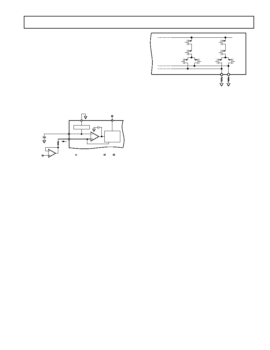
Figure 21 shows the equivalent analog output circuit of the
AD9754 consisting of a parallel combination of PMOS differen-
tial current switches associated with each segmented current
source. The output impedance of IOUTA and IOUTB is deter-
mined by the equivalent parallel combination of the PMOS
switches and is typically 100 k
in parallel with 5 pF. Due to
the nature of a PMOS device, the output impedance is also
slightly dependent on the output voltage (i.e., VOUTA and VOUTB)
and, to a lesser extent, the analog supply voltage, AVDD, and
full-scale current, IOUTFS. Although the output impedance’s signal
dependency can be a source of dc nonlinearity and ac linearity
(i.e., distortion), its effects can be limited if certain precautions
are noted.
AD9754
AVDD
IOUTA
IOUTB
RLOAD
Figure 21. Equivalent Analog Output Circuit
IOUTA and IOUTB also have a negative and positive voltage
compliance range. The negative output compliance range of
–1.0 V is set by the breakdown limits of the CMOS process.
Operation beyond this maximum limit may result in a break-
down of the output stage and affect the reliability of the AD9754.
The positive output compliance range is slightly dependent on
the full-scale output current, IOUTFS. It degrades slightly from its
nominal 1.25 V for an IOUTFS = 20 mA to 1.00 V for an IOUTFS =
2 mA. Operation beyond the positive compliance range will
induce clipping of the output signal which severely degrades
the AD9754’s linearity and distortion performance.
For applications requiring the optimum dc linearity, IOUTA
and/or IOUTB should be maintained at a virtual ground via an
I-V op amp configuration. Maintaining IOUTA and/or IOUTB
at a virtual ground keeps the output impedance of the AD9754
fixed, significantly reducing its effect on linearity. However,
it does not necessarily lead to the optimum distortion perfor-
mance due to limitations of the I-V op amp. Note that the
INL/DNL specifications for the AD9754 are measured in
this manner using IOUTA. In addition, these dc linearity
specifications remain virtually unaffected over the specified
power supply range of +4.5 V to +5.5 V.
Operating the AD9754 with reduced voltage output swings at
IOUTA and IOUTB in a differential or single-ended output
configuration reduces the signal dependency of its output
impedance thus enhancing distortion performance. Although
the voltage compliance range of IOUTA and IOUTB extends
from –1.0 V to +1.25 V, optimum distortion performance is
achieved when the maximum full-scale signal at IOUTA and
IOUTB does not exceed approximately 0.5 V. A properly se-
lected transformer with a grounded center-tap will allow the
AD9754 to provide the required power and voltage levels to
different loads while maintaining reduced voltage swings at
IOUTA and IOUTB. DC-coupled applications requiring a
differential or single-ended output configuration should size
RLOAD accordingly. Refer to Applying the AD9754 section for
examples of various output configurations.
相关PDF资料 |
PDF描述 |
|---|---|
| CS3108A-32-25PW | CONN PLUG 25POS RT ANG W/PINS |
| VE-JTX-MZ-F3 | CONVERTER MOD DC/DC 5.2V 25W |
| MS27505E17F55SB | CONN RCPT 55POS BOX MNT W/SCKT |
| MS3452W36-15S | CONN RCPT 35POS BOX MNT W/SCKT |
| VE-JTX-MZ-F2 | CONVERTER MOD DC/DC 5.2V 25W |
相关代理商/技术参数 |
参数描述 |
|---|---|
| AD9754ARZ | 功能描述:IC DAC 14BIT 125MSPS 28-SOIC RoHS:是 类别:集成电路 (IC) >> 数据采集 - 数模转换器 系列:TxDAC® 标准包装:1 系列:- 设置时间:4.5µs 位数:12 数据接口:串行,SPI? 转换器数目:1 电压电源:单电源 功率耗散(最大):- 工作温度:-40°C ~ 125°C 安装类型:表面贴装 封装/外壳:8-SOIC(0.154",3.90mm 宽) 供应商设备封装:8-SOICN 包装:剪切带 (CT) 输出数目和类型:1 电压,单极;1 电压,双极 采样率(每秒):* 其它名称:MCP4921T-E/SNCTMCP4921T-E/SNRCTMCP4921T-E/SNRCT-ND |
| AD9754ARZ | 制造商:Analog Devices 功能描述:IC 14BIT DAC POLY FUSE SMD 9754 |
| AD9754ARZRL | 功能描述:IC DAC 14BIT 125MSPS 28-SOIC TR RoHS:是 类别:集成电路 (IC) >> 数据采集 - 数模转换器 系列:TxDAC® 标准包装:47 系列:- 设置时间:2µs 位数:14 数据接口:并联 转换器数目:1 电压电源:单电源 功率耗散(最大):55µW 工作温度:-40°C ~ 85°C 安装类型:表面贴装 封装/外壳:28-SSOP(0.209",5.30mm 宽) 供应商设备封装:28-SSOP 包装:管件 输出数目和类型:1 电流,单极;1 电流,双极 采样率(每秒):* |
| AD9754-EB | 制造商:Analog Devices 功能描述:Evaluation Board For AD9754 制造商:Analog Devices 功能描述:DEV TOOLS, EVAL BD FOR AD9754 - Bulk |
| AD9754-EBZ | 功能描述:BOARD EVAL FOR AD9754 RoHS:是 类别:编程器,开发系统 >> 评估板 - 数模转换器 (DAC) 系列:TxDAC® 产品培训模块:Lead (SnPb) Finish for COTS Obsolescence Mitigation Program 标准包装:1 系列:- DAC 的数量:4 位数:12 采样率(每秒):- 数据接口:串行,SPI? 设置时间:3µs DAC 型:电流/电压 工作温度:-40°C ~ 85°C 已供物品:板 已用 IC / 零件:MAX5581 |
发布紧急采购,3分钟左右您将得到回复。