参数资料
| 型号: | AD9754ARUZRL7 |
| 厂商: | Analog Devices Inc |
| 文件页数: | 7/24页 |
| 文件大小: | 0K |
| 描述: | IC DAC 14BIT 125MSPS 28-TSSOP |
| 产品培训模块: | Data Converter Fundamentals DAC Architectures |
| 标准包装: | 1,000 |
| 系列: | TxDAC® |
| 设置时间: | 35ns |
| 位数: | 14 |
| 数据接口: | 并联 |
| 转换器数目: | 1 |
| 电压电源: | 模拟和数字 |
| 功率耗散(最大): | 220mW |
| 工作温度: | -40°C ~ 85°C |
| 安装类型: | 表面贴装 |
| 封装/外壳: | 28-TSSOP(0.173",4.40mm 宽) |
| 供应商设备封装: | 28-TSSOP |
| 包装: | 带卷 (TR) |
| 输出数目和类型: | 1 电流,单极;1 电流,双极 |
| 采样率(每秒): | 125M |
| 其它名称: | AD9754ARUZRL7-ND AD9754ARUZRL7TR |
AD9754
–15–
REV. A
SINGLE-ENDED UNBUFFERED VOLTAGE OUTPUT
Figure 30 shows the AD9754 configured to provide a unipolar
output range of approximately 0 V to +0.5 V for a doubly termi-
nated 50
cable since the nominal full-scale current, I
OUTFS, of
20 mA flows through the equivalent RLOAD of 25
. In this case,
RLOAD represents the equivalent load resistance seen by IOUTA
or IOUTB. The unused output (IOUTA or IOUTB) can be
connected to ACOM directly or via a matching RLOAD. Different
values of IOUTFS and RLOAD can be selected as long as the posi-
tive compliance range is adhered to. One additional consider-
ation in this mode is the integral nonlinearity (INL) as discussed
in the Analog Output section of this data sheet. For optimum
INL performance, the single-ended, buffered voltage output
configuration is suggested.
AD9754
IOUTA
IOUTB 21
50
25
50
VOUTA = 0 TO +0.5V
IOUTFS = 20mA
22
Figure 30. 0 V to +0.5 V Unbuffered Voltage Output
SINGLE-ENDED BUFFERED VOLTAGE OUTPUT
CONFIGURATION
Figure 31 shows a buffered single-ended output configuration in
which the op amp U1 performs an I-V conversion on the AD9754
output current. U1 maintains IOUTA (or IOUTB) at a virtual
ground, thus minimizing the nonlinear output impedance effect
on the DAC’s INL performance as discussed in the Analog
Output section. Although this single-ended configuration typi-
cally provides the best dc linearity performance, its ac distortion
performance at higher DAC update rates may be limited by
U1’s slewing capabilities. U1 provides a negative unipolar
output voltage and its full-scale output voltage is simply the
product of RFB and IOUTFS. The full-scale output should be set
within U1’s voltage output swing capabilities by scaling IOUTFS
and/or RFB. An improvement in ac distortion performance may
result with a reduced IOUTFS since the signal current U1 will be
required to sink will be subsequently reduced.
AD9754
22
IOUTA
IOUTB 21
COPT
200
U1
VOUT = IOUTFS
RFB
IOUTFS = 10mA
RFB
200
Figure 31. Unipolar Buffered Voltage Output
POWER AND GROUNDING CONSIDERATIONS, POWER
SUPPLY REJECTION
Many applications seek high speed and high performance under
less than ideal operating conditions. In these circuits, the imple-
mentation and construction of the printed circuit board design
is as important as the circuit design. Proper RF techniques must
be used for device selection, placement and routing as well as
power supply bypassing and grounding to ensure optimum
performance. Figures 39-44 illustrate the recommended printed
circuit board ground, power and signal plane layouts which are
implemented on the AD9754 evaluation board.
One factor that can measurably affect system performance is the
ability of the DAC output to reject dc variations or ac noise
superimposed on the analog or digital dc power distribution
(i.e., AVDD, DVDD). This is referred to as Power Supply
Rejection Ratio (PSRR). For dc variations of the power supply,
the resulting performance of the DAC directly corresponds to a
gain error associated with the DAC’s full-scale current, IOUTFS.
AC noise on the dc supplies is common in applications where
the power distribution is generated by a switching power supply.
Typically, switching power supply noise will occur over the
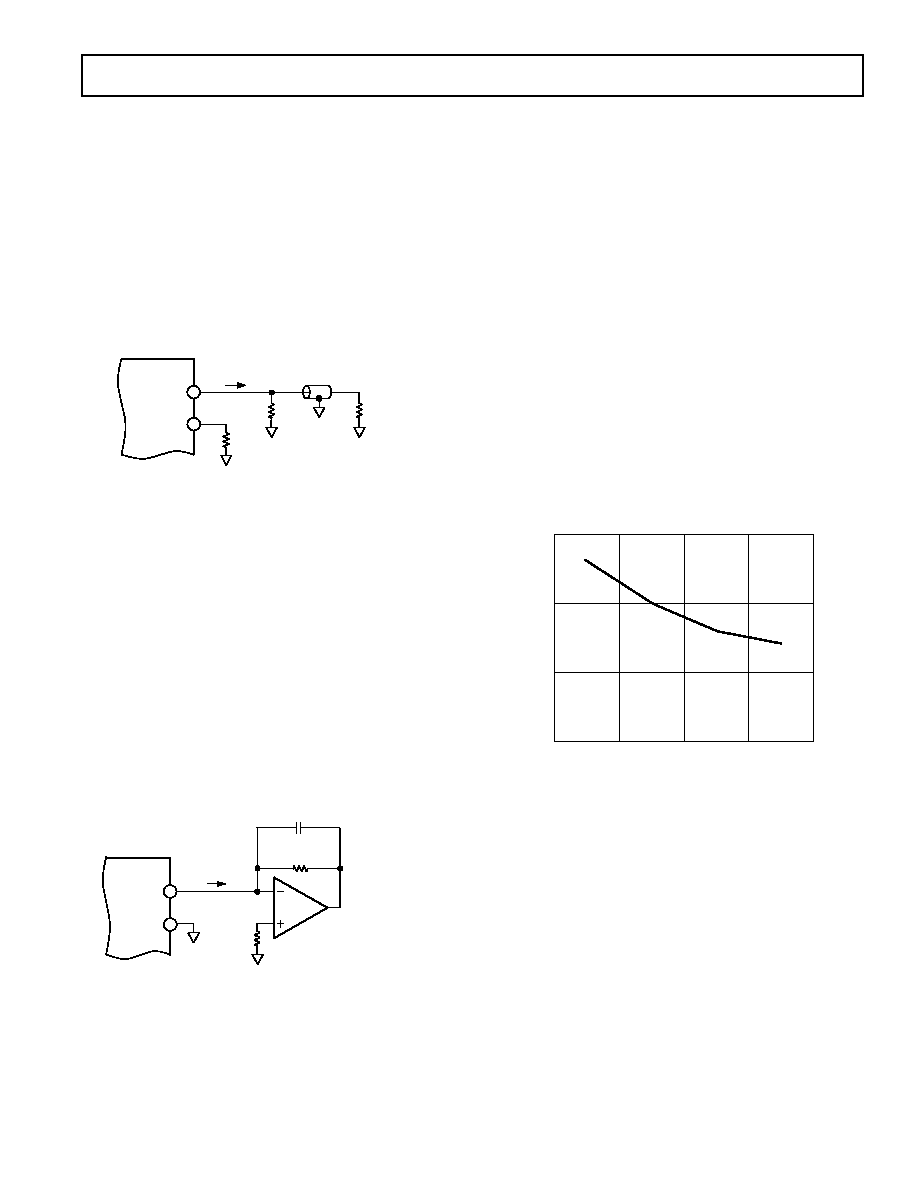
spectrum from tens of kHz to several MHz. PSRR vs. frequency
of the AD9754 AVDD supply, over this frequency range, is
given in Figure 32.
FREQUENCY – MHz
PSRR
–
dB
90
60
1.0
0.5
0.75
80
70
0.26
Figure 32. Power Supply Rejection Ratio of AD9754
Note that the units in Figure 32 are given in units of (amps out)/
(volts in). Noise on the analog power supply has the effect of
modulating the internal switches, and therefore the output
current. The voltage noise on the dc power, therefore, will be
added in a nonlinear manner to the desired IOUT. Due to the
relative different sizes of these switches, PSRR is very code
dependent. This can produce a mixing effect which can modu-
late low frequency power supply noise to higher frequencies.
Worst case PSRR for either one of the differential DAC outputs
will occur when the full-scale current is directed towards that
output. As a result, the PSRR measurement in Figure 32 repre-
sents a worst case condition in which the digital inputs remain
static and the full-scale output current of 20 mA is directed to
the DAC output being measured.
相关PDF资料 |
PDF描述 |
|---|---|
| CS3108A-32-25PW | CONN PLUG 25POS RT ANG W/PINS |
| VE-JTX-MZ-F3 | CONVERTER MOD DC/DC 5.2V 25W |
| MS27505E17F55SB | CONN RCPT 55POS BOX MNT W/SCKT |
| MS3452W36-15S | CONN RCPT 35POS BOX MNT W/SCKT |
| VE-JTX-MZ-F2 | CONVERTER MOD DC/DC 5.2V 25W |
相关代理商/技术参数 |
参数描述 |
|---|---|
| AD9754ARZ | 功能描述:IC DAC 14BIT 125MSPS 28-SOIC RoHS:是 类别:集成电路 (IC) >> 数据采集 - 数模转换器 系列:TxDAC® 标准包装:1 系列:- 设置时间:4.5µs 位数:12 数据接口:串行,SPI? 转换器数目:1 电压电源:单电源 功率耗散(最大):- 工作温度:-40°C ~ 125°C 安装类型:表面贴装 封装/外壳:8-SOIC(0.154",3.90mm 宽) 供应商设备封装:8-SOICN 包装:剪切带 (CT) 输出数目和类型:1 电压,单极;1 电压,双极 采样率(每秒):* 其它名称:MCP4921T-E/SNCTMCP4921T-E/SNRCTMCP4921T-E/SNRCT-ND |
| AD9754ARZ | 制造商:Analog Devices 功能描述:IC 14BIT DAC POLY FUSE SMD 9754 |
| AD9754ARZRL | 功能描述:IC DAC 14BIT 125MSPS 28-SOIC TR RoHS:是 类别:集成电路 (IC) >> 数据采集 - 数模转换器 系列:TxDAC® 标准包装:47 系列:- 设置时间:2µs 位数:14 数据接口:并联 转换器数目:1 电压电源:单电源 功率耗散(最大):55µW 工作温度:-40°C ~ 85°C 安装类型:表面贴装 封装/外壳:28-SSOP(0.209",5.30mm 宽) 供应商设备封装:28-SSOP 包装:管件 输出数目和类型:1 电流,单极;1 电流,双极 采样率(每秒):* |
| AD9754-EB | 制造商:Analog Devices 功能描述:Evaluation Board For AD9754 制造商:Analog Devices 功能描述:DEV TOOLS, EVAL BD FOR AD9754 - Bulk |
| AD9754-EBZ | 功能描述:BOARD EVAL FOR AD9754 RoHS:是 类别:编程器,开发系统 >> 评估板 - 数模转换器 (DAC) 系列:TxDAC® 产品培训模块:Lead (SnPb) Finish for COTS Obsolescence Mitigation Program 标准包装:1 系列:- DAC 的数量:4 位数:12 采样率(每秒):- 数据接口:串行,SPI? 设置时间:3µs DAC 型:电流/电压 工作温度:-40°C ~ 85°C 已供物品:板 已用 IC / 零件:MAX5581 |
发布紧急采购,3分钟左右您将得到回复。