- 您现在的位置:买卖IC网 > PDF目录17102 > AD9761-EBZ (Analog Devices Inc)BOARD EVAL FOR AD9761 PDF资料下载
参数资料
| 型号: | AD9761-EBZ |
| 厂商: | Analog Devices Inc |
| 文件页数: | 6/24页 |
| 文件大小: | 0K |
| 描述: | BOARD EVAL FOR AD9761 |
| 产品培训模块: | DAC Architectures |
| 标准包装: | 1 |
| 系列: | TxDAC® |
| DAC 的数量: | 2 |
| 位数: | 10 |
| 采样率(每秒): | 40M |
| 数据接口: | 并联 |
| 设置时间: | 35ns |
| DAC 型: | 电流 |
| 工作温度: | -40°C ~ 85°C |
| 已供物品: | 板 |
| 已用 IC / 零件: | AD9761 |
| 相关产品: | AD9761ARSZRL-ND - IC DAC 10BIT DUAL 40MSPS 28-SSOP AD9761ARSZ-ND - IC DAC 10BIT DUAL 40MSPS 28-SSOP AD9761ARSRL-ND - IC DAC 10BIT DUAL 40MSPS 28-SSOP AD9761ARS-ND - IC DAC 10BIT DUAL 40MSPS 28-SSOP |
AD9761
–14–
AD9761
–15–
result, the digital inputs can also accommodate TTL levels
when DVDD is set to accommodate the maximum high
level voltage, VOH(MAX), of the TTL drivers. A DVDD of 3 V
to 3.3 V will typically ensure proper compatibility of most
TTL logic families. Figure 13 shows the equivalent digital
input circuit for the data, sleep, and clock inputs.
RESET
DATA
SELECT
CLOCK/WRITE
I0
Q0
I1
Q1
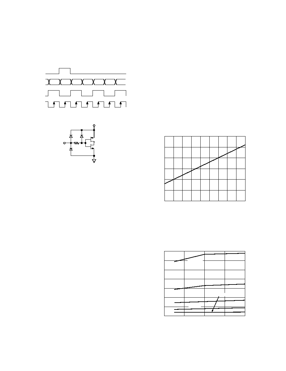
Figure 12.Timing Diagram
DVDD
DIGITAL
INPUT
Figure 13. Equivalent Digital Input
Since the AD9761 is capable of being updated up to 40 MSPS,
the quality of the clock and data input signals are important
in achieving the optimum performance. The drivers of the
digital data interface circuitry should be specified to meet
the minimum setup and hold times of the AD9761 as well
as its required min/max input logic level thresholds. The
external clock driver circuitry should provide the AD9761
with a low jitter clock input meeting the min/max logic
levels while providing fast edges. Fast clock edges will help
minimize any jitter that can manifest itself as phase noise
on a reconstructed waveform.
Digital signal paths should be kept short, and run lengths
matched to avoid propagation delay mismatch. The inser-
tion of a low value resistor network (i.e., 20 to 100 )
between the AD9761 digital inputs and driver outputs
may be helpful in reducing any overshooting and ringing at
the digital inputs, which contributes to data feedthrough.
Operating the AD9761 with reduced logic swings and a
corresponding digital supply (DVDD) will also reduce data
feedthrough.
RESET/SLEEP MODE OPERATION
The RESET/SLEEP input can be used either to power down
the AD9761 or reset its internal digital interface logic. If the
RESET/SLEEP input is asserted for greater than one clock
cycle but under four clock cycles by applying a Logic 1, the
internal state machine will be reset. If the RESET/SLEEP input
is asserted for four clock cycles or longer, the power-down func-
tion of the AD9761 will be initiated. The power-down function
turns off the output current and reduces the supply current to
less than 9 mA over the specified supply range of 3 V to 5.5 V
and temperature range.
The power-up and power-down characteristics of the AD9761
are dependent upon the value of the compensation
capacitor connected to COMP1 and COMP3. With a
nominal value of 0.1 F, the AD9761 takes less than 5 s to
power down and approximately 3.25 ms to power back up.
POWER DISSIPATION
The power dissipation of the AD9761 is dependent on several
factors, including
1. AVDD and DVDD, the power supply voltages.
2. IOUTFS, the full-scale current output.
3. fCLOCK, the update rate.
4. The reconstructed digital input waveform.
The power dissipation is directly proportional to the analog
supply current, IAVDD, and the digital supply current, IDVDD.
IAVDD is directly proportional to IOUTFS, as shown in Fig-
ure 14, and is insensitive to fCLOCK.
IOUTFS (mA)
30
0
1
10
2
3
4
5
6
7
8
9
25
20
15
10
5
I AVDD
(m
A
)
Figure 14. IAVDD vs. IOUTFS
Conversely, IDVDD is dependent on both the digital input
waveform, fCLOCK, and digital supply, DVDD. Figures 15
and 16 show IDVDD as a function of a full-scale sine wave
output ratio’s (fOUT/fCLOCK) for various update rates with
DVDD = 5 V and DVDD = 3 V, respectively.
5MSPS
RATIO (fOUT/fCLK)
40
30
0.05
0.15
40MSPS
20
0
0.10
20MSPS
10MSPS
10
0
I DVDD
(mA
)
0.20
50
60
70
2.5MSPS
Figure 15. IDVDD vs. Ratio @ DVDD = 5 V
REV. C
相关PDF资料 |
PDF描述 |
|---|---|
| DC1485A | BOARD DAC LTC2757 |
| RCM15DTKI-S288 | CONN EDGECARD 30POS .156 EXTEND |
| RCM15DTMD-S189 | CONN EDGECARD 30POS R/A .156 SLD |
| 0210390987 | CABLE JUMPER 1MM .030M 29POS |
| AD9742ACP-PCBZ | BOARD EVAL FOR AD9742ACP |
相关代理商/技术参数 |
参数描述 |
|---|---|
| AD9762 | 制造商:AD 制造商全称:Analog Devices 功能描述:Analog Devices: Data Converters: DAC 12-Bit, 10 ns to 100 ns Converters Selection Table |
| AD9762AR | 功能描述:IC DAC 12BIT 125MSPS 28-SOIC RoHS:否 类别:集成电路 (IC) >> 数据采集 - 数模转换器 系列:TxDAC® 产品培训模块:Data Converter Fundamentals DAC Architectures 标准包装:750 系列:- 设置时间:7µs 位数:16 数据接口:并联 转换器数目:1 电压电源:双 ± 功率耗散(最大):100mW 工作温度:0°C ~ 70°C 安装类型:表面贴装 封装/外壳:28-LCC(J 形引线) 供应商设备封装:28-PLCC(11.51x11.51) 包装:带卷 (TR) 输出数目和类型:1 电压,单极;1 电压,双极 采样率(每秒):143k |
| AD9762ARRL | 功能描述:IC DAC 12BIT 100KSPS 28-SOIC RoHS:否 类别:集成电路 (IC) >> 数据采集 - 数模转换器 系列:TxDAC® 标准包装:47 系列:- 设置时间:2µs 位数:14 数据接口:并联 转换器数目:1 电压电源:单电源 功率耗散(最大):55µW 工作温度:-40°C ~ 85°C 安装类型:表面贴装 封装/外壳:28-SSOP(0.209",5.30mm 宽) 供应商设备封装:28-SSOP 包装:管件 输出数目和类型:1 电流,单极;1 电流,双极 采样率(每秒):* |
| AD9762ARU | 功能描述:IC DAC 12BIT 125MSPS 28-TSSOP RoHS:否 类别:集成电路 (IC) >> 数据采集 - 数模转换器 系列:TxDAC® 产品培训模块:Data Converter Fundamentals DAC Architectures 标准包装:750 系列:- 设置时间:7µs 位数:16 数据接口:并联 转换器数目:1 电压电源:双 ± 功率耗散(最大):100mW 工作温度:0°C ~ 70°C 安装类型:表面贴装 封装/外壳:28-LCC(J 形引线) 供应商设备封装:28-PLCC(11.51x11.51) 包装:带卷 (TR) 输出数目和类型:1 电压,单极;1 电压,双极 采样率(每秒):143k |
发布紧急采购,3分钟左右您将得到回复。