- 您现在的位置:买卖IC网 > PDF目录17102 > AD9761-EBZ (Analog Devices Inc)BOARD EVAL FOR AD9761 PDF资料下载
参数资料
| 型号: | AD9761-EBZ |
| 厂商: | Analog Devices Inc |
| 文件页数: | 8/24页 |
| 文件大小: | 0K |
| 描述: | BOARD EVAL FOR AD9761 |
| 产品培训模块: | DAC Architectures |
| 标准包装: | 1 |
| 系列: | TxDAC® |
| DAC 的数量: | 2 |
| 位数: | 10 |
| 采样率(每秒): | 40M |
| 数据接口: | 并联 |
| 设置时间: | 35ns |
| DAC 型: | 电流 |
| 工作温度: | -40°C ~ 85°C |
| 已供物品: | 板 |
| 已用 IC / 零件: | AD9761 |
| 相关产品: | AD9761ARSZRL-ND - IC DAC 10BIT DUAL 40MSPS 28-SSOP AD9761ARSZ-ND - IC DAC 10BIT DUAL 40MSPS 28-SSOP AD9761ARSRL-ND - IC DAC 10BIT DUAL 40MSPS 28-SSOP AD9761ARS-ND - IC DAC 10BIT DUAL 40MSPS 28-SSOP |
AD9761
–16–
AD9761
–17–
The differential circuit shown in Figure 19 provides the neces-
sary level-shifting required in a single-supply system. In this
case, AVDD, which is the positive analog supply for both the
AD9761 and the op amp, is also used to level-shift the differ-
ential output of the AD9761 to midsupply (i.e., AVDD/2).
COPT
200
1k
IOUTA
IOUTB
AD9761
RLOAD
50
200
AD8042
500
RLOAD
50
1k
AVDD
Figure 19. Single-Supply DC Differential Coupled
Circuit
Single-Ended Unbuffered Voltage Output
Figure 20 shows the AD9761 configured to provide a uni-
polar output range of approximately 0 V to 0.5 V since the
nominal full-scale current, IOUTFS, of 10 mA flows through an
RLOAD of 50 . In the case of a doubly terminated low-pass
filter, RLOAD represents the equivalent load resistance seen by
IOUTA or IOUTB. The unused output (IOUTA or IOUTB)
can be connected to ACOM directly or via a matching RLOAD.
Different values of IOUTFS and RLOAD can be selected as long
as the positive compliance range is adhered to.
50
IOUTA
IOUTB
AD9761
50
IOUTFS = 10mA
VOUT =
0V TO 0.5V
Figure 20. 0 V to 0.5 V Unbuffered Voltage Output
Differential, DC-Coupled Output Configuration with
Level Shifting
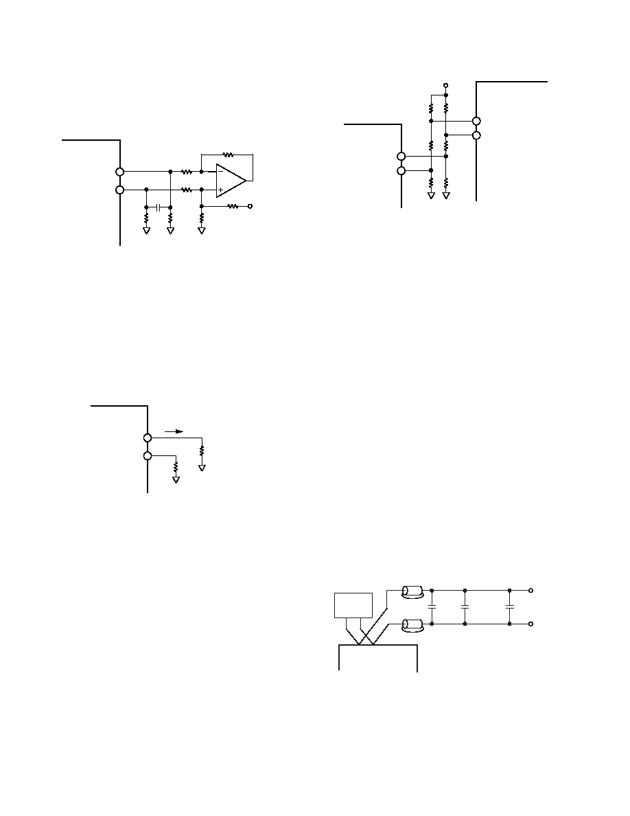
Some applications may require the AD9761 differential outputs
to interface to a single-supply quadrature upconverter.
Although most of these devices provide differential inputs,
its common-mode voltage range does not typically extend
to ground. As a result, the ground-referenced output signals
shown in Figure 20 must be level shifted to within the
specified common-mode range of the single-supply quadrature
upconverter. Figure 21 shows the addition of a resistor pull-up
network that provides the level shifting function. The use
of matched resistor networks will maintain maximum gain
matching and minimum offset performance between the
I and Q channels. Note, the resistor pull-up network will
introduce approximately 6 dB of signal attenuation.
50**
IOUTA
IOUTB
AD9761
50**
500*
AVDD
VIN+
VIN–
QUADRATURE
UPCONVERTER
*OHMTEK TO MC-1603-5000D
**OHMTEK TO MC-1603-1000D
Figure 21. Differential, DC-Coupled Output
Configuration with Level-Shifting
POWER AND GROUNDING CONSIDERATIONS
In systems seeking to simultaneously achieve high speed and
high performance, the implementation and construction of
the printed circuit board design is often as important as the
circuit design. Proper RF techniques must be used in device
selection, placement and routing, and supply bypassing and
grounding. The evaluation board for the AD9761, which
uses a 4-layer PC board, serves as a good example for the
previously mentioned considerations. The evaluation board
provides an illustration of the recommended printed circuit
board ground, power, and signal plane layout.
Proper grounding and decoupling should be a primary objec-
tive in any high speed, high resolution system. The AD9761
features separate analog and digital supply and ground pins
to optimize the management of analog and digital ground
currents in a system. In general, AVDD, the analog supply,
should be decoupled to ACOM, the analog common, as
close to the chip as physically possible. Similarly, DVDD,
the digital supply should be decoupled as close to DCOM as
physically as possible.
For those applications requiring a single 5 V or 3.3 V supply
for both the analog and digital supply, a clean analog supply
may be generated using the circuit shown in Figure 22.
The circuit consists of a differential LC filter with separate
power supply and return lines. Lower noise can be attained
using low ESR type electrolytic and tantalum capacitors.
0.1F
CER.
10F–22F
TANT.
100F
ELECT.
AVDD
ACOM
+
–
FERRITE
BEADS
5V OR 3V POWER
SUPPLY
TTL/CMOS
LOGIC
CIRCUITS
Figure 22. Differential LC Filter for Single 5 V or 3 V
Applications
REV. C
相关PDF资料 |
PDF描述 |
|---|---|
| DC1485A | BOARD DAC LTC2757 |
| RCM15DTKI-S288 | CONN EDGECARD 30POS .156 EXTEND |
| RCM15DTMD-S189 | CONN EDGECARD 30POS R/A .156 SLD |
| 0210390987 | CABLE JUMPER 1MM .030M 29POS |
| AD9742ACP-PCBZ | BOARD EVAL FOR AD9742ACP |
相关代理商/技术参数 |
参数描述 |
|---|---|
| AD9762 | 制造商:AD 制造商全称:Analog Devices 功能描述:Analog Devices: Data Converters: DAC 12-Bit, 10 ns to 100 ns Converters Selection Table |
| AD9762AR | 功能描述:IC DAC 12BIT 125MSPS 28-SOIC RoHS:否 类别:集成电路 (IC) >> 数据采集 - 数模转换器 系列:TxDAC® 产品培训模块:Data Converter Fundamentals DAC Architectures 标准包装:750 系列:- 设置时间:7µs 位数:16 数据接口:并联 转换器数目:1 电压电源:双 ± 功率耗散(最大):100mW 工作温度:0°C ~ 70°C 安装类型:表面贴装 封装/外壳:28-LCC(J 形引线) 供应商设备封装:28-PLCC(11.51x11.51) 包装:带卷 (TR) 输出数目和类型:1 电压,单极;1 电压,双极 采样率(每秒):143k |
| AD9762ARRL | 功能描述:IC DAC 12BIT 100KSPS 28-SOIC RoHS:否 类别:集成电路 (IC) >> 数据采集 - 数模转换器 系列:TxDAC® 标准包装:47 系列:- 设置时间:2µs 位数:14 数据接口:并联 转换器数目:1 电压电源:单电源 功率耗散(最大):55µW 工作温度:-40°C ~ 85°C 安装类型:表面贴装 封装/外壳:28-SSOP(0.209",5.30mm 宽) 供应商设备封装:28-SSOP 包装:管件 输出数目和类型:1 电流,单极;1 电流,双极 采样率(每秒):* |
| AD9762ARU | 功能描述:IC DAC 12BIT 125MSPS 28-TSSOP RoHS:否 类别:集成电路 (IC) >> 数据采集 - 数模转换器 系列:TxDAC® 产品培训模块:Data Converter Fundamentals DAC Architectures 标准包装:750 系列:- 设置时间:7µs 位数:16 数据接口:并联 转换器数目:1 电压电源:双 ± 功率耗散(最大):100mW 工作温度:0°C ~ 70°C 安装类型:表面贴装 封装/外壳:28-LCC(J 形引线) 供应商设备封装:28-PLCC(11.51x11.51) 包装:带卷 (TR) 输出数目和类型:1 电压,单极;1 电压,双极 采样率(每秒):143k |
发布紧急采购,3分钟左右您将得到回复。