参数资料
| 型号: | AD9762ARZRL |
| 厂商: | Analog Devices Inc |
| 文件页数: | 5/23页 |
| 文件大小: | 0K |
| 描述: | IC DAC 12BIT 125MSPS 28-SOIC |
| 产品培训模块: | Data Converter Fundamentals DAC Architectures |
| 标准包装: | 1,000 |
| 系列: | TxDAC® |
| 设置时间: | 35ns |
| 位数: | 12 |
| 数据接口: | 并联 |
| 转换器数目: | 1 |
| 电压电源: | 模拟和数字 |
| 功率耗散(最大): | 160mW |
| 工作温度: | -40°C ~ 85°C |
| 安装类型: | 表面贴装 |
| 封装/外壳: | 28-SOIC(0.295",7.50mm 宽) |
| 供应商设备封装: | 28-SOIC W |
| 包装: | 带卷 (TR) |
| 输出数目和类型: | 2 电流,单极;2 电流,双极 |
| 采样率(每秒): | 125M |
AD9762
–13–
REV. B
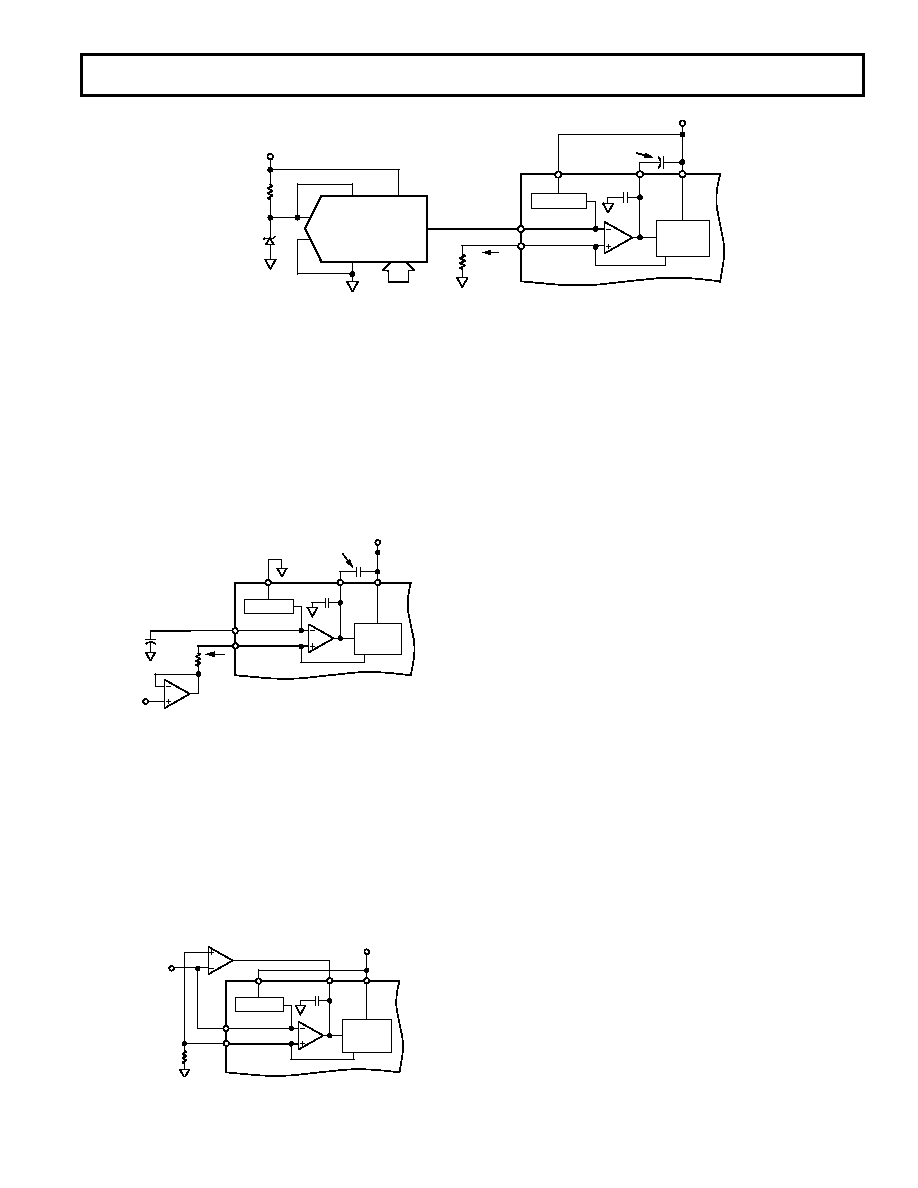
The second method may be used in a dual-supply system in
which the common-mode voltage of REFIO is fixed and IREF is
varied by an external voltage, VGC, applied to RSET via an ampli-
fier. An example of this method is shown in Figure 44 in which
the internal reference is used to set the common-mode voltage
of the control amplifier to 1.20 V. The external voltage, VGC, is
referenced to ACOM and should not exceed 1.2 V. The value
of RSET is such that IREFMAX and IREFMIN do not exceed 62.5
A
and 625
A, respectively. The associated equations in Figure 44
can be used to determine the value of RSET.
50pF
COMP1
+1.2V REF
AVDD
REFLO
CURRENT
SOURCE
ARRAY
AVDD
REFIO
FS ADJ
RSET
AD9762
IREF
OPTIONAL
BANDLIMITING
CAPACITOR
VGC
1 F
IREF = (1.2–VGC)/RSET
WITH VGC < VREFIO AND 62.5 A
IREF
625A
Figure 44. Dual-Supply Gain Control Circuit
In some applications, the user may elect to use an external con-
trol amplifier to enhance the multiplying bandwidth, distortion
performance, and/or settling time. External amplifiers capable
of driving a 50 pF load such as the AD817 are suitable for this
purpose. It is configured in such a way that it is in parallel with
the weaker internal reference amplifier as shown in Figure 45.
In this case, the external amplifier simply overdrives the weaker
reference control amplifier. Also, since the internal control
amplifier has a limited current output, it will sustain no damage
if overdriven.
50pF
COMP1
+1.2V REF
AVDD
REFLO
CURRENT
SOURCE
ARRAY
AVDD
REFIO
FS ADJ
RSET
AD9762
VREF
INPUT
EXTERNAL
CONTROL AMPLIFIER
Figure 45. Configuring an External Reference Control
Amplifier
ANALOG OUTPUTS
The AD9762 produces two complementary current outputs,
IOUTA and IOUTB, which may be configured for single-ended or
differential operation. IOUTA and IOUTB can be converted into
complementary single-ended voltage outputs, VOUTA and VOUTB,
via a load resistor, RLOAD, as described in the DAC Transfer
Function section by Equations 5 through 8. The differential
voltage, VDIFF, existing between VOUTA and VOUTB can also be
converted to a single-ended voltage via a transformer or differ-
ential amplifier configuration. The ac performance of the
AD9762 is optimum and specified using a differential trans-
former coupled output in which the voltage swing at IOUTA and
IOUTB is limited to
±0.5 V. If a single-ended unipolar output is
desirable, IOUTA should be selected.
The distortion and noise performance of the AD9762 can be
enhanced when the AD9762 is configured for differential opera-
tion. The common-mode error sources of both IOUTA and IOUTB
can be significantly reduced by the common-mode rejection of a
transformer or differential amplifier. These common-mode
error sources include even-order distortion products and noise.
The enhancement in distortion performance becomes more
significant as the frequency content of the reconstructed wave-
form increases. This is due to the first order cancellation of
various dynamic common-mode distortion mechanisms, digital
feedthrough and noise.
Performing a differential-to-single-ended conversion via a
transformer also provides the ability to deliver twice the recon-
structed signal power to the load (i.e., assuming no source
termination). Since the output currents of IOUTA and IOUTB are
complementary, they become additive when processed differen-
tially. A properly selected transformer will allow the AD9762 to
provide the required power and voltage levels to different loads.
Refer to Applying the AD9762 section for examples of various
output configurations.
The output impedance of IOUTA and IOUTB is determined by the
equivalent parallel combination of the PMOS switches associ-
ated with the current sources and is typically 100 k
in parallel
with 5 pF. It is also slightly dependent on the output voltage
(i.e., VOUTA and VOUTB) due to the nature of a PMOS device.
As a result, maintaining IOUTA and/or IOUTB at a virtual ground
via an I-V op amp configuration will result in the optimum dc
linearity. Note, the INL/DNL specifications for the AD9762
are measured with IOUTA maintained at a virtual ground via an
op amp.
1.2V
50pF
COMP1
+1.2V REF
AVDD
REFLO
CURRENT
SOURCE
ARRAY
AVDD
REFIO
FS ADJ
RSET
AD9762
IREF =
VREF/RSET
AVDD
OPTIONAL
BANDLIMITING
CAPACITOR
VREF
VDD
RFB
OUT1
OUT2
AGND
DB7–DB0
AD7524
AD1580
0.1V TO 1.2V
Figure 43. Single-Supply Gain Control Circuit
相关PDF资料 |
PDF描述 |
|---|---|
| VI-J0K-MX-B1 | CONVERTER MOD DC/DC 40V 75W |
| VI-J0J-MX-B1 | CONVERTER MOD DC/DC 36V 75W |
| IDT49FCT3805SO | IC CLK BUFFER 1:5 100MHZ 20-SOIC |
| V110A24H400BL3 | CONVERTER MOD DC/DC 24V 400W |
| IDT49FCT3805QI8 | IC CLK BUFFER 1:5 100MHZ 20-QSOP |
相关代理商/技术参数 |
参数描述 |
|---|---|
| AD9762-EB | 制造商:Analog Devices 功能描述:IC SEMICONDUCTOR ((NS)) |
| AD9762-EBZ | 功能描述:BOARD EVAL FOR AD9762 RoHS:是 类别:编程器,开发系统 >> 评估板 - 数模转换器 (DAC) 系列:TxDAC® 产品培训模块:Lead (SnPb) Finish for COTS Obsolescence Mitigation Program 标准包装:1 系列:- DAC 的数量:4 位数:12 采样率(每秒):- 数据接口:串行,SPI? 设置时间:3µs DAC 型:电流/电压 工作温度:-40°C ~ 85°C 已供物品:板 已用 IC / 零件:MAX5581 |
| AD9763 | 制造商:AD 制造商全称:Analog Devices 功能描述:10-Bit, 125 MSPS Dual TxDAC+ D/A Converter |
| AD9763_11 | 制造商:AD 制造商全称:Analog Devices 功能描述:10-/12-/14-Bit, 125 MSPS Dual TxDAC Digital-to-Analog Converters |
| AD9763AST | 制造商:Analog Devices 功能描述:DAC 2-CH Segment 10-bit 48-Pin LQFP 制造商:Rochester Electronics LLC 功能描述:10 BIT, 125 MSPS DUAL TXDAC+ - Tape and Reel 制造商:Analog Devices 功能描述:IC 10-BIT DAC |
发布紧急采购,3分钟左右您将得到回复。