参数资料
| 型号: | AD9762ARZRL |
| 厂商: | Analog Devices Inc |
| 文件页数: | 7/23页 |
| 文件大小: | 0K |
| 描述: | IC DAC 12BIT 125MSPS 28-SOIC |
| 产品培训模块: | Data Converter Fundamentals DAC Architectures |
| 标准包装: | 1,000 |
| 系列: | TxDAC® |
| 设置时间: | 35ns |
| 位数: | 12 |
| 数据接口: | 并联 |
| 转换器数目: | 1 |
| 电压电源: | 模拟和数字 |
| 功率耗散(最大): | 160mW |
| 工作温度: | -40°C ~ 85°C |
| 安装类型: | 表面贴装 |
| 封装/外壳: | 28-SOIC(0.295",7.50mm 宽) |
| 供应商设备封装: | 28-SOIC W |
| 包装: | 带卷 (TR) |
| 输出数目和类型: | 2 电流,单极;2 电流,双极 |
| 采样率(每秒): | 125M |
AD9762
–15–
REV. B
IOUTFS – mA
30
0
220
4
6
8
10
121416
18
25
20
15
10
5
I AVDD
–
mA
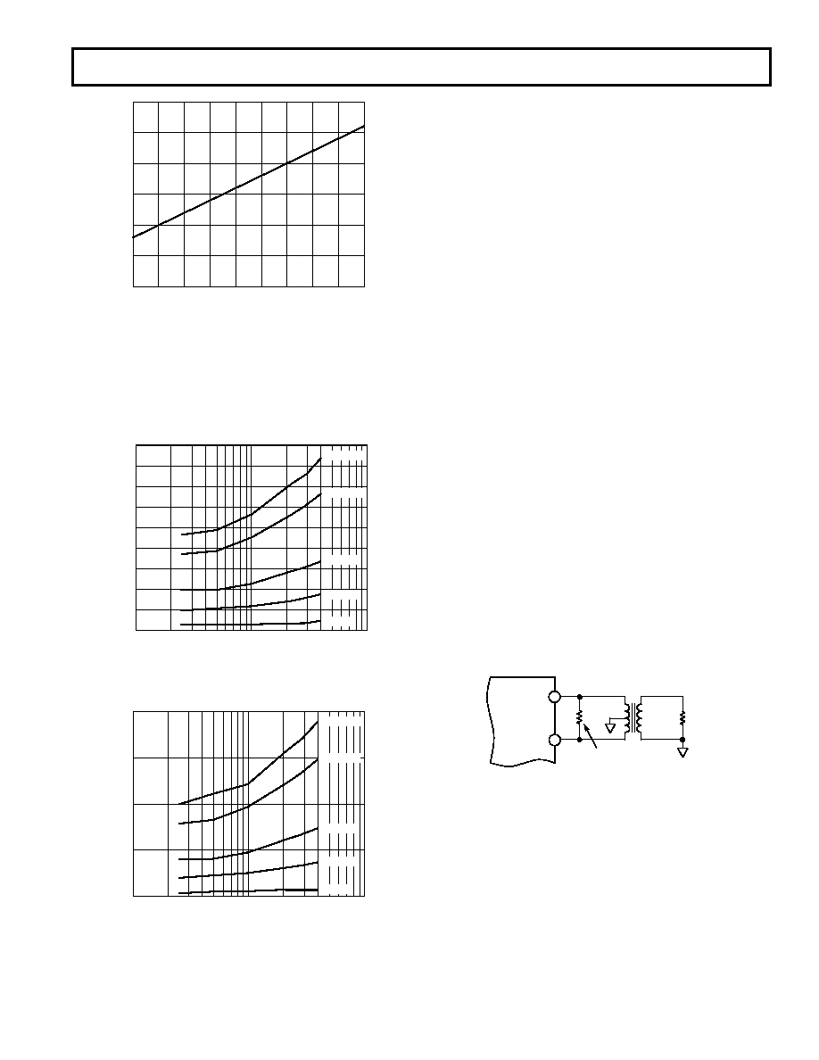
Figure 47. IAVDD vs. IOUTFS
Conversely, IDVDD is dependent on both the digital input wave-
form, fCLOCK, and digital supply DVDD. Figures 48 and 49
show IDVDD as a function of full-scale sine wave output ratios
(fOUT/fCLOCK) for various update rates with DVDD = 5 V and
DVDD = 3 V, respectively. Note, how IDVDD is reduced by more
than a factor of 2 when DVDD is reduced from 5 V to 3 V.
RATIO (fOUT/fCLK)
18
16
0
0.01
1
0.1
I DVDD
–
mA
8
6
4
2
12
10
14
5MSPS
25MSPS
50MSPS
100MSPS
125MSPS
Figure 48. IDVDD vs. Ratio @ DVDD = 5 V
RATIO (fOUT/fCLK)
8
0
0.01
1
0.1
I DVDD
–
mA
6
4
2
5MSPS
25MSPS
50MSPS
100MSPS
125MSPS
Figure 49. IDVDD vs. Ratio @ DVDD = 3 V
APPLYING THE AD9762
OUTPUT CONFIGURATIONS
The following sections illustrate some typical output configura-
tions for the AD9762. Unless otherwise noted, it is assumed
that IOUTFS is set to a nominal 20 mA. For applications requir-
ing the optimum dynamic performance, a differential output
configuration is suggested. A differential output configuration
may consist of either an RF transformer or a differential op amp
configuration. The transformer configuration provides the
optimum high frequency performance and is recommended for
any application allowing for ac coupling. The differential op
amp configuration is suitable for applications requiring dc
coupling, a bipolar output, signal gain and/or level shifting.
A single-ended output is suitable for applications requiring a
unipolar voltage output. A positive unipolar output voltage will
result if IOUTA and/or IOUTB is connected to an appropriately
sized load resistor, RLOAD, referred to ACOM. This configura-
tion may be more suitable for a single-supply system requiring
a dc coupled, ground referred output voltage. Alternatively, an
amplifier could be configured as an I-V converter thus converting
IOUTA or IOUTB into a negative unipolar voltage. This configura-
tion provides the best dc linearity since IOUTA or IOUTB is
maintained at a virtual ground. Note, IOUTA provides slightly
better performance than IOUTB.
DIFFERENTIAL COUPLING USING A TRANSFORMER
An RF transformer can be used to perform a differential-to-
single-ended signal conversion as shown in Figure 50. A
differentially coupled transformer output provides the optimum
distortion performance for output signals whose spectral content
lies within the transformer’s passband. An RF transformer such
as the Mini-Circuits T1-1T provides excellent rejection of
common-mode distortion (i.e., even-order harmonics) and noise
over a wide frequency range. It also provides electrical isolation
and the ability to deliver twice the power to the load. Trans-
formers with different impedance ratios may also be used for
impedance matching purposes. Note that the transformer
provides ac coupling only.
RLOAD
AD9762
22
21
MINI-CIRCUITS
T1-1T
OPTIONAL RDIFF
IOUTA
IOUTB
Figure 50. Differential Output Using a Transformer
The center tap on the primary side of the transformer must be
connected to ACOM to provide the necessary dc current path
for both IOUTA and IOUTB. The complementary voltages appear-
ing at IOUTA and IOUTB (i.e., VOUTA and VOUTB) swing symmetri-
cally around ACOM and should be maintained with the specified
output compliance range of the AD9762. A differential resistor,
RDIFF, may be inserted in applications in which the output of
the transformer is connected to the load, RLOAD, via a passive
reconstruction filter or cable. RDIFF is determined by the
transformer’s impedance ratio and provides the proper source
termination which results in a low VSWR. Note that approxi-
mately half the signal power will be dissipated across RDIFF.
相关PDF资料 |
PDF描述 |
|---|---|
| VI-J0K-MX-B1 | CONVERTER MOD DC/DC 40V 75W |
| VI-J0J-MX-B1 | CONVERTER MOD DC/DC 36V 75W |
| IDT49FCT3805SO | IC CLK BUFFER 1:5 100MHZ 20-SOIC |
| V110A24H400BL3 | CONVERTER MOD DC/DC 24V 400W |
| IDT49FCT3805QI8 | IC CLK BUFFER 1:5 100MHZ 20-QSOP |
相关代理商/技术参数 |
参数描述 |
|---|---|
| AD9762-EB | 制造商:Analog Devices 功能描述:IC SEMICONDUCTOR ((NS)) |
| AD9762-EBZ | 功能描述:BOARD EVAL FOR AD9762 RoHS:是 类别:编程器,开发系统 >> 评估板 - 数模转换器 (DAC) 系列:TxDAC® 产品培训模块:Lead (SnPb) Finish for COTS Obsolescence Mitigation Program 标准包装:1 系列:- DAC 的数量:4 位数:12 采样率(每秒):- 数据接口:串行,SPI? 设置时间:3µs DAC 型:电流/电压 工作温度:-40°C ~ 85°C 已供物品:板 已用 IC / 零件:MAX5581 |
| AD9763 | 制造商:AD 制造商全称:Analog Devices 功能描述:10-Bit, 125 MSPS Dual TxDAC+ D/A Converter |
| AD9763_11 | 制造商:AD 制造商全称:Analog Devices 功能描述:10-/12-/14-Bit, 125 MSPS Dual TxDAC Digital-to-Analog Converters |
| AD9763AST | 制造商:Analog Devices 功能描述:DAC 2-CH Segment 10-bit 48-Pin LQFP 制造商:Rochester Electronics LLC 功能描述:10 BIT, 125 MSPS DUAL TXDAC+ - Tape and Reel 制造商:Analog Devices 功能描述:IC 10-BIT DAC |
发布紧急采购,3分钟左右您将得到回复。