参数资料
| 型号: | AD9765ASTZ |
| 厂商: | Analog Devices Inc |
| 文件页数: | 19/44页 |
| 文件大小: | 0K |
| 描述: | IC DAC 12BIT DUAL 125MSPS 48LQFP |
| 产品培训模块: | Data Converter Fundamentals DAC Architectures |
| 标准包装: | 1 |
| 系列: | TxDAC+® |
| 设置时间: | 35ns |
| 位数: | 12 |
| 数据接口: | 并联 |
| 转换器数目: | 2 |
| 电压电源: | 模拟和数字 |
| 功率耗散(最大): | 450mW |
| 工作温度: | -40°C ~ 85°C |
| 安装类型: | 表面贴装 |
| 封装/外壳: | 48-LQFP |
| 供应商设备封装: | 48-LQFP(7x7) |
| 包装: | 托盘 |
| 输出数目和类型: | 4 电流,单极;4 电流,双极 |
| 采样率(每秒): | 125M |
| 产品目录页面: | 785 (CN2011-ZH PDF) |
| 配用: | AD9765-EBZ-ND - BOARD EVAL FOR AD9765 |
第1页第2页第3页第4页第5页第6页第7页第8页第9页第10页第11页第12页第13页第14页第15页第16页第17页第18页当前第19页第20页第21页第22页第23页第24页第25页第26页第27页第28页第29页第30页第31页第32页第33页第34页第35页第36页第37页第38页第39页第40页第41页第42页第43页第44页
AD9763/AD9765/AD9767
Data Sheet
Rev. G | Page 26 of 44
Because the AD9763/AD9765/AD9767 is capable of being clocked
up to 125 MSPS, the quality of the clock and data input signals
are important in achieving the optimum performance. Operating
the AD9763/AD9765/AD9767 with reduced logic swings and a
corresponding digital supply (DVDD1/DVDD2) results in the
lowest data feedthrough and on-chip digital noise. The drivers of
the digital data interface circuitry should be specified to meet the
minimum setup and hold times of the AD9763/AD9765/AD9767
as well as its required minimum and maximum input logic level
thresholds.
Digital signal paths should be kept short, and run lengths should be
matched to avoid propagation delay mismatch. The insertion
of a low value (that is, 20 Ω to 100 Ω) resistor network between
the AD9763/AD9765/AD9767 digital inputs and driver outputs
can be helpful in reducing any overshooting and ringing at the
digital inputs that contribute to digital feedthrough. For longer
board traces and high data update rates, stripline techniques
with proper impedance and termination resistors should be
considered to maintain “clean” digital inputs.
The external clock driver circuitry provides the AD9763/AD9765/
AD9767 with a low-jitter clock input meeting the minimum
and maximum logic levels while providing fast edges. Fast clock
edges help minimize jitter manifesting itself as phase noise on a
reconstructed waveform. Therefore, the clock input should be
driven by the fastest logic family suitable for the application.
Note that the clock input can also be driven via a sine wave, which
is centered around the digital threshold (that is, DVDDx/2) and
meets the minimum and maximum logic threshold. This
typically results in a slight degradation in the phase noise, which
becomes more noticeable at higher sampling rates and output
frequencies. In addition, at higher sampling rates, the 20%
tolerance of the digital logic threshold should be considered,
because it affects the effective clock duty cycle and,
subsequently, cuts into the required data setup and hold times.
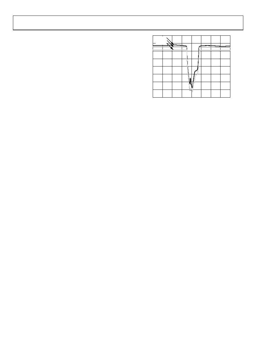
Input Clock and Data Timing Relationship
SNR in a DAC is dependent on the relationship between the
position of the clock edges and the point in time at which the
input data changes. The AD9763/AD9765/AD9767 are rising
edge triggered and therefore exhibit SNR sensitivity when the
data transition is close to this edge. The goal when applying the
AD9763/AD9765/AD9767 is to make the data transition close
to the falling clock edge. This becomes more important as the
sample rate increases. Figure 68 shows the relationship of SNR
to clock placement with different sample rates. Note that at the
lower sample rates, much more tolerance is allowed in clock
placement; much more care must be taken at higher rates.
80
70
60
50
40
30
20
10
0
–4
–3
–2
–1
0
1
2
3
4
SN
R
(
d
B
c)
TIME OF DATA CHANGE RELATIVE TO
RISING CLOCK EDGE (ns)
AD9763
AD9765
AD9767
00
61
7-
06
8
Figure 68. SNR vs. Clock Placement @ fOUT = 20 MHz and fCLK = 125 MSPS
SLEEP MODE OPERATION
The AD9763/AD9765/AD9767 has a power-down function that
turns off the output current and reduces the supply current to less
than 8.5 mA over the specified supply range of 3.3 V to 5 V and
over the full operating temperature range. This mode can be
activated by applying a Logic Level 1 to the SLEEP pin. The
SLEEP pin logic threshold is equal to 0.5 × AVDD. This digital
input also contains an active pull-down circuit that ensures the
AD9763/AD9765/AD9767 remains enabled if this input is left
disconnected. The AD9763/AD9765/AD9767 require less than
50 ns to power down and approximately 5 μs to power back up.
POWER DISSIPATION
The power dissipation (PD) of the AD9763/AD9765/AD9767 is
dependent on several factors, including
the power supply voltages (AVDD and DVDD1/DVDD2)
the full-scale current output (IOUTFS)
the update rate (fCLK)
the reconstructed digital input waveform
The power dissipation is directly proportional to the analog
supply current (IAVDD) and the digital supply current (IDVDD).
and is insensitive to fCLK.
Conversely, IDVDD is dependent on the digital input waveform,
output ratios (fOUT/fCLK) for various update rates with DVDD1 =
DVDD2 = 5 V and DVDD1 = DVDD2 = 3.3 V, respectively. Note
that IDVDD is reduced by more than a factor of 2 when
DVDD1/DVDD2 is reduced from 5 V to 3.3 V.
相关PDF资料 |
PDF描述 |
|---|---|
| MS3120F16-8S | CONN RCPT 8POS WALL MNT W/SCKT |
| VI-J4B-MZ-F1 | CONVERTER MOD DC/DC 95V 25W |
| VI-24Z-MU-F1 | CONVERTER MOD DC/DC 2V 80W |
| MS27468T25F19PC | CONN RCPT 19POS JAM NUT W/PINS |
| VI-J1L-MZ-F4 | CONVERTER MOD DC/DC 28V 25W |
相关代理商/技术参数 |
参数描述 |
|---|---|
| AD9765ASTZ | 制造商:Analog Devices 功能描述:12BIT DAC DUAL 125MSPS 48LQFP 制造商:Analog Devices 功能描述:12BIT DAC, DUAL, 125MSPS, 48LQFP |
| AD9765ASTZKL1 | 制造商:Rochester Electronics LLC 功能描述: 制造商:Analog Devices 功能描述: |
| AD9765ASTZRL | 功能描述:IC DAC 12BIT DUAL 125MSPS 48LQFP RoHS:是 类别:集成电路 (IC) >> 数据采集 - 数模转换器 系列:TxDAC+® 产品培训模块:Data Converter Fundamentals DAC Architectures 标准包装:750 系列:- 设置时间:7µs 位数:16 数据接口:并联 转换器数目:1 电压电源:双 ± 功率耗散(最大):100mW 工作温度:0°C ~ 70°C 安装类型:表面贴装 封装/外壳:28-LCC(J 形引线) 供应商设备封装:28-PLCC(11.51x11.51) 包装:带卷 (TR) 输出数目和类型:1 电压,单极;1 电压,双极 采样率(每秒):143k |
| AD9765-EB | 制造商:Analog Devices 功能描述: |
| AD9765-EBZ | 功能描述:BOARD EVAL FOR AD9765 RoHS:是 类别:编程器,开发系统 >> 评估板 - 数模转换器 (DAC) 系列:TxDAC+® 产品培训模块:Lead (SnPb) Finish for COTS Obsolescence Mitigation Program 标准包装:1 系列:- DAC 的数量:4 位数:12 采样率(每秒):- 数据接口:串行,SPI? 设置时间:3µs DAC 型:电流/电压 工作温度:-40°C ~ 85°C 已供物品:板 已用 IC / 零件:MAX5581 |
发布紧急采购,3分钟左右您将得到回复。