- 您现在的位置:买卖IC网 > PDF目录17064 > AD9767-EBZ (Analog Devices Inc)BOARD EVAL FOR AD9767 PDF资料下载
参数资料
| 型号: | AD9767-EBZ |
| 厂商: | Analog Devices Inc |
| 文件页数: | 17/44页 |
| 文件大小: | 0K |
| 描述: | BOARD EVAL FOR AD9767 |
| 产品培训模块: | DAC Architectures |
| 标准包装: | 1 |
| 系列: | TxDAC+® |
| DAC 的数量: | 2 |
| 位数: | 14 |
| 采样率(每秒): | 125M |
| 数据接口: | 并联 |
| 设置时间: | 35ns |
| DAC 型: | 电流 |
| 工作温度: | -40°C ~ 85°C |
| 已供物品: | 板 |
| 已用 IC / 零件: | AD9767 |
| 相关产品: | AD9767ASTZRL-ND - IC DAC 14BIT DUAL 125MSPS 48LQFP AD9767ASTZ-ND - IC DAC 14BIT DUAL 125MSPS 48LQFP |
第1页第2页第3页第4页第5页第6页第7页第8页第9页第10页第11页第12页第13页第14页第15页第16页当前第17页第18页第19页第20页第21页第22页第23页第24页第25页第26页第27页第28页第29页第30页第31页第32页第33页第34页第35页第36页第37页第38页第39页第40页第41页第42页第43页第44页
AD9763/AD9765/AD9767
Data Sheet
Rev. G | Page 24 of 44
IOUTA and IOUTB also have a negative and positive voltage
compliance range that must be adhered to in order to achieve
optimum performance. The negative output compliance range
of 1.0 V is set by the breakdown limits of the CMOS process.
Operation beyond this maximum limit may result in a breakdown
of the output stage and affect the reliability of the
AD9763/AD9765/AD9767.
The positive output compliance range is slightly dependent on
the full-scale output current, IOUTFS. When IOUTFS is decreased
from 20 mA to 2 mA, the positive output compliance range
degrades slightly from its nominal 1.25 V to 1.00 V. The optimum
distortion performance for a single-ended or differential output
is achieved when the maximum full-scale signal at IOUTA and IOUTB
does not exceed 0.5 V. Applications requiring the AD9763/
AD9765/AD9767 output (that is, VOUTA and/or VOUTB) to extend its
output compliance range must size RLOAD accordingly. Operation
beyond this compliance range adversely affects the linearity
performance of the AD9763/AD9765/AD9767 and
subsequently degrades its distortion performance.
DIGITAL INPUTS
The digital inputs of the AD9763/AD9765/AD9767 consist of
two independent channels. For the dual-port mode, each DAC has
its own dedicated 10-/12-/14-bit data port: WRT line and CLK line.
In the interleaved timing mode, the function of the digital control
pins changes as described in the Interleaved Mode Timing
section. The 10-/12-/14-bit parallel data inputs follow straight
binary coding, where the most significant bits (MSBs) are DB9P1
and DB9P2 for the AD9763, DB11P1 and DB11P2 for the AD9765,
and DB13P1 and DB13P2 for the AD9767, and the least significant
bits (LSBs) are DB0P1 and DB0P2 for all three parts. IOUTA produces
a full-scale output current when all data bits are at Logic 1. IOUTB
produces a complementary output with the full-scale current
split between the two outputs as a function of the input code.
The digital interface is implemented using an edge-triggered
master/slave latch. The DAC outputs are updated following
either the rising edge or every other rising edge of the clock,
depending on whether dual or interleaved mode is used. The
DAC outputs are designed to support a clock rate as high as
125 MSPS. The clock can be operated at any duty cycle that
meets the specified latch pulse width. The setup and hold times
can also be varied within the clock cycle as long as the specified
minimum times are met, although the location of these transition
edges may affect digital feedthrough and distortion performance.
Best performance is typically achieved when the input data
transitions on the falling edge of a 50% duty cycle clock.
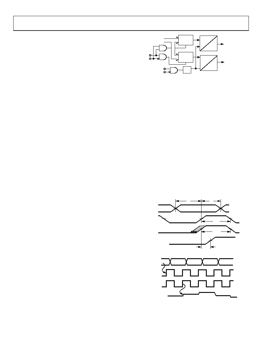
DAC TIMING
The AD9763/AD9765/AD9767 can operate in two timing modes,
dual and interleaved, which are described in the following
sections. The block diagram in Figure 61 represents the latch
architecture in the interleaved timing mode.
IQSEL
IQWRT
DAC1
INTERLEAVED
DATA IN, PORT 1
IQCLK
IQRESET
DAC2
÷2
PORT 1
INPUT
LATCH
PORT 2
INPUT
LATCH
DEINTERLEAVED
DATA OUT
DAC1
LATCH
DAC2
LATCH
00
61
7-
0
61
Figure 61. Latch Structure in Interleaved Mode
Dual-Port Mode Timing
When the MODE pin is at Logic 1, the AD9763/AD9765/AD9767
operates in dual-port mode (refer to Figure 57). The AD9763/
AD9765/AD9767 functions as two distinct DACs. Each DAC
has its own completely independent digital input and control lines.
The AD9763/AD9765/AD9767 features a double-buffered data
path. Data enters the device through the channel input latches.
This data is then transferred to the DAC latch in each signal
path. After the data is loaded into the DAC latch, the analog
output settles to its new value.
For general consideration, the WRT lines control the channel
input latches, and the CLK lines control the DAC latches. Both
sets of latches are updated on the rising edge of their respective
control signals.
The rising edge of CLK must occur before or simultaneously
with the rising edge of WRT. If the rising edge of CLK occurs
after the rising edge of WRT, a minimum delay of 2 ns must be
maintained from the rising edge of WRT to the rising edge of CLK.
Timing specifications for dual-port mode are shown in Figure 62
and Figure 63.
DATA IN
WRT1/WRT2
CLK1/CLK2
tPD
IOUTA
OR
IOUTB
tS
tH
tLPW
tCPW
00
61
7-
0
62
Figure 62. Dual-Port Mode Timing
DATA IN
WRT1/WRT2
CLK1/CLK2
XX
D1
D2
D3
D4
IOUTA
OR
IOUTB
D1
D2
D3
D4
D5
00
61
7-
06
3
Figure 63. Dual-Port Mode Timing
相关PDF资料 |
PDF描述 |
|---|---|
| 0210490255 | CABLE JUMPER 1.25MM .030M 20POS |
| MLG1005S2N0S | INDUCTOR MULTILAYER 2.0NH 0402 |
| MIC2003-0.5YML TR | IC DISTRIBUTION SW 0.5A 6-MLF |
| MIC2005-0.5YM6 TR | IC DISTRIBUTION SW 0.5A SOT23-6 |
| 0210490204 | CABLE JUMPER 1.25MM .203M 14POS |
相关代理商/技术参数 |
参数描述 |
|---|---|
| AD9768 | 制造商:AD 制造商全称:Analog Devices 功能描述:Ultrahigh Speed IC D/A Converter |
| AD9768JD | 制造商:Rochester Electronics LLC 功能描述:AD9768 IC - Bulk |
| AD9768JQ | 制造商:Rochester Electronics LLC 功能描述:- Bulk |
| AD9768SD | 制造商:AD 制造商全称:Analog Devices 功能描述:Ultrahigh Speed IC D/A Converter |
| AD9768SE | 制造商:Rochester Electronics LLC 功能描述:- Bulk |
发布紧急采购,3分钟左右您将得到回复。