- 您现在的位置:买卖IC网 > PDF目录17063 > AD9779A-DPG2-EBZ (Analog Devices Inc)BOARD EVALUATION FOR AD9779A PDF资料下载
参数资料
| 型号: | AD9779A-DPG2-EBZ |
| 厂商: | Analog Devices Inc |
| 文件页数: | 41/56页 |
| 文件大小: | 0K |
| 描述: | BOARD EVALUATION FOR AD9779A |
| 设计资源: | Interfacing ADL5370 to AD9779A Dual-Channel, 1 GSPS High Speed DAC (CN0016) Interfacing ADL5371 to AD9779A Dual-Channel, 1 GSPS High Speed DAC (CN0017) Interfacing ADL5372 to AD9779A Dual-Channel, 1 GSPS High Speed DAC (CN0018) Interfacing ADL5373 to AD9779A Dual-Channel, 1 GSPS High Speed DAC (CN0019) Interfacing ADL5374 to AD9779A Dual-Channel, 1 GSPS High Speed DAC (CN0020) Interfacing ADL5375 to AD9779A Dual-Channel, 1 GSPS High Speed DAC (CN0021) AD9788-79A Eval Brd Schematic AD9779A-DPG2-EBZ BOM AD9779A-DPG2-EBZ Gerber Files |
| 标准包装: | 1 |
| 系列: | * |
| DAC 的数量: | 2 |
| 位数: | 16 |
| 采样率(每秒): | 1G |
| 数据接口: | 串行 |
| DAC 型: | 电流 |
| 工作温度: | -40°C ~ 85°C |
| 已供物品: | * |
| 已用 IC / 零件: | AD9779A |
第1页第2页第3页第4页第5页第6页第7页第8页第9页第10页第11页第12页第13页第14页第15页第16页第17页第18页第19页第20页第21页第22页第23页第24页第25页第26页第27页第28页第29页第30页第31页第32页第33页第34页第35页第36页第37页第38页第39页第40页当前第41页第42页第43页第44页第45页第46页第47页第48页第49页第50页第51页第52页第53页第54页第55页第56页
AD9776A/AD9778A/AD9779A
Rev. B | Page 46 of 56
INPUT DATA PORTS
DUAL PORT MODE
The AD9776A/AD9778A/AD9779A can operate in two data
input modes: dual port mode and single port mode. For the
default dual port mode (single port bit = 0), each DAC receives
data from a dedicated input port. In single port mode (single
port bit = 1), both DACs receive data from Port 1. In single port
mode, DAC1 and DAC2 data is interleaved, and the TXENABLE
input is used to steer data to the intended DAC. In dual port
mode, the TXENABLE input is used to power down the digital
data path.
In dual port mode, data for each DAC is received on the
respective input bus (P1D[15:0] or P2D[15:0]). I and Q data
arrive simultaneously and are sampled on the rising edge of the
DATACLK signal. The TXENABLE signal must be high to enable
the transmit path.
INPUT DATA REFERENCED TO DATACLK
The simplest method of interfacing to the AD9776A/AD9778A/
AD9779A is when the input data is referenced to the DATACLK
output. The DATACLK output is a buffered version (with some
fixed delay) of the internal clock that is used to latch the input
data. Therefore, if setup and hold times of the input data with
respect to DATACLK are met, the input data is latched correctly.
Detailed timing diagrams for the single and dual port cases
using DATACLK as the timing reference are shown in Figure 82.
In dual port mode, the data must be delivered at the input data
rate. In single port mode, data must be delivered at twice the
input data rate of each DAC. Because the data inputs function
up to a maximum of 300 MSPS, it is practical to operate with
input data rates up to 150 MHz per DAC in single port mode.
In dual port and single port modes, a data clock output
(DATACLK) signal is available as a fixed time base with which
to drive data from an FPGA or other data source. This output
signal operates at the input data rate.
DATACLK
DATA
tSDATACLK
tHDATACLK
064
52
-30
8
SINGLE PORT MODE
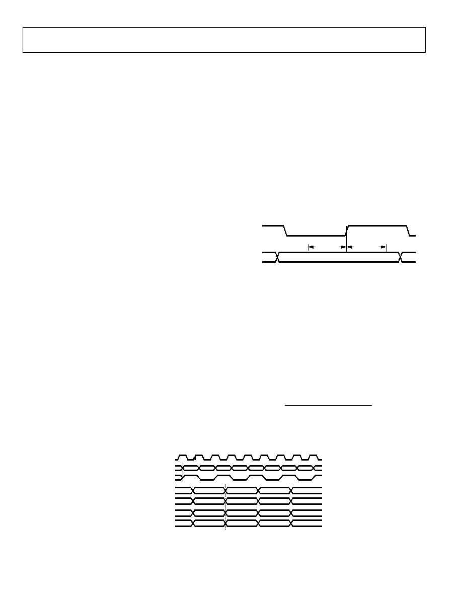
In single port mode, data for both DACs is received on the Port 1
input bus (P1D[15:0]). I and Q data samples are interleaved and
are sampled on the rising edges of DATACLK. Along with the
data, a framing signal must be supplied on the TXENABLE
input (Pin 39), which steers incoming data to its respective DAC.
When TXENABLE is high, the corresponding data-word is sent
to the I DAC. When TXENABLE is low, the corresponding data is
sent to the Q DAC. The timing of the digital interface in
interleaved mode is shown in Figure 83.
Figure 82. Input Data Port Timing, Data Referenced to DATACLK
Table 28 shows the setup and hold time requirements for the
input data over the operating temperature range of the device.
Also shown is the keep out window (KOW). The keep out
window is the sum of the setup and hold times of the interface.
This is the minimum amount of time valid data must be
presented to the device to ensure proper sampling.
DATACLK Frequency Settings
The DATACLK signal is derived from the internal DAC sample
clock, DACCLK. The frequency of the DATACLK output depends
on several programmable settings. Normally, the frequency of
DATACLK is equal to the input data rate. The relationship
between the frequency of DACCLK and DATACLK is
The Q first bit (Register 0x02, Bit 0) controls the pairing order
of the input data. With the Q first bit set to the default of 0, the
I-Q pairing sent to the DACs is the two input data-words
corresponding to TXENABLE low followed by TXENABLE
high. With the Q first bit set to 1, the I-Q pairing sent to the
DACs is the two input data-words corresponding to TXENABLE
high, followed by TXENABLE low. Note that with either order
pairing, the data sent with TXENABLE high is directed to the
I DAC, and the data sent with TXENABLE low is directed to the
Q DAC.
DATACLKDIV
SP
ZS
IF
f
DACCLK
DATACLK
×
=
where the variables IF, ZS, SP, and DATACLKDIV have the
values shown in Table 27.
06
45
2-
30
6
DATACLK
P1D[15:0]
TXENABLE
I DAC[15:0]
Q DAC[15:0]
I DAC[15:0]
Q DAC[15:0]
Q FIRST = 1
Q FIRST = 0
P1D1
P1D2
P1D3
P1D4
P1D5
P1D6
P1D7
P1D8
P1D1
P1D3
P1D5
P1D1
P1D0
P1D3
P1D5
P1D2
P1D4
P1D6
P1D2
P1D4
Figure 83. Single Port Mode Digital Interface Timing
相关PDF资料 |
PDF描述 |
|---|---|
| DC955A | BOARD DELTA SIGMA ADC LTC2483 |
| SDR0604-181KL | INDUCTOR POWER 180UH 0.38A SMD |
| AP2186SG-13 | IC USB PWR SWITCH 1.5A DUAL 8SOP |
| AD9755-EB | BOARD EVAL FOR AD9755 |
| HBM11DRYI-S13 | CONN EDGECARD 22POS .156 EXTEND |
相关代理商/技术参数 |
参数描述 |
|---|---|
| AD9779A-EBZ | 制造商:Analog Devices 功能描述:DUAL 16B, 1.0 GSPS TXDAC - Bulk |
| AD9779AMOD-EBZ | 制造商:Analog Devices 功能描述:DUAL 16B, 1.0 GSPS TXDAC - Bulk |
| AD9779AXSVZ | 制造商:Analog Devices 功能描述:DUAL 16-BIT, 1 GSPS, DIGITAL-TO-ANALOG CONVERTER - Bulk |
| AD9779BSV | 制造商:Analog Devices 功能描述:DAC 2CH INTERPOLATION FLTR 16BIT 100TQFP EP - Bulk |
| AD9779BSVZ | 功能描述:IC DAC 16BIT DUAL 1GSPS 100TQFP RoHS:是 类别:集成电路 (IC) >> 数据采集 - 数模转换器 系列:- 产品培训模块:Lead (SnPb) Finish for COTS Obsolescence Mitigation Program 标准包装:1,000 系列:- 设置时间:1µs 位数:8 数据接口:串行 转换器数目:8 电压电源:双 ± 功率耗散(最大):941mW 工作温度:0°C ~ 70°C 安装类型:表面贴装 封装/外壳:24-SOIC(0.295",7.50mm 宽) 供应商设备封装:24-SOIC W 包装:带卷 (TR) 输出数目和类型:8 电压,单极 采样率(每秒):* |
发布紧急采购,3分钟左右您将得到回复。