- 您现在的位置:买卖IC网 > PDF目录10075 > AD977ABRSZRL (Analog Devices Inc)IC ADC 16BIT 200KSPS 28SSOP PDF资料下载
参数资料
| 型号: | AD977ABRSZRL |
| 厂商: | Analog Devices Inc |
| 文件页数: | 10/24页 |
| 文件大小: | 0K |
| 描述: | IC ADC 16BIT 200KSPS 28SSOP |
| 标准包装: | 1,500 |
| 位数: | 16 |
| 采样率(每秒): | 200k |
| 数据接口: | 串行,SPI? |
| 转换器数目: | 1 |
| 功率耗散(最大): | 100mW |
| 电压电源: | 模拟和数字 |
| 工作温度: | -40°C ~ 85°C |
| 安装类型: | 表面贴装 |
| 封装/外壳: | 28-SSOP(0.209",5.30mm 宽) |
| 供应商设备封装: | 28-SSOP |
| 包装: | 带卷 (TR) |
| 输入数目和类型: | 3 个单端,单极;3 个单端,双极 |
| 配用: | EVAL-AD977CB-ND - BOARD EVAL FOR AD977 EVAL-AD977ACB-ND - BOARD EVAL FOR AD977A |
AD977/AD977A
–18–
REV. D
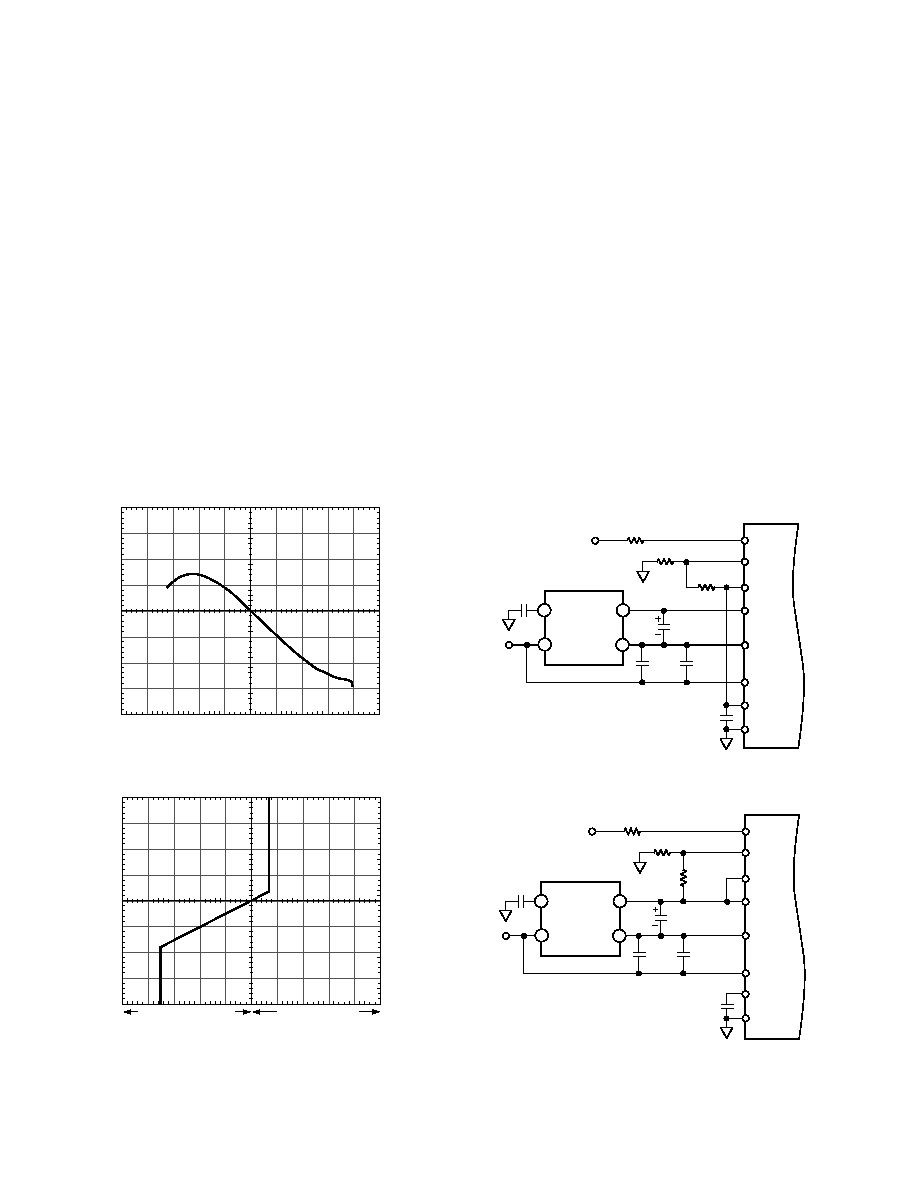
VOLTAGE REFERENCE
The AD977/AD977A has an on-chip temperature compensated
bandgap voltage reference that is factory trimmed to 2.5 V
±20 mV. The accuracy of the AD977/AD977A over the speci-
fied temperature ranges is dominated by the drift performance
of the voltage reference. The on-chip voltage reference is laser-
trimmed to provide a typical drift of 7 ppm/
°C. This typical drift
characteristic is shown in Figure 14, which is a plot of the
change in reference voltage (in mV) versus the change in tem-
perature—notice the plot is normalized for zero error at 25
°C.
If improved drift performance is required, an external reference
such as the AD780 should be used to provide a drift as low as
3 ppm/
°C. In order to simplify the drive requirements of the
voltage reference (internal or external), an onboard reference
buffer is provided. The output of this buffer is provided at the
CAP pin and is available to the user; however, when externally
loading the reference buffer, it is important to make sure that
proper precautions are taken to minimize any degradation in the
ADC’s performance. Figure 15 shows the load regulation of the
reference buffer. Notice that this figure is also normalized so
that there is zero error with no dc load. In the linear region, the
output impedance at this point is typically 1
. Because of this
1
output impedance, it is important to minimize any ac or
DEGREES CELSIUS
–55
1mV/DIV
25
125
Figure 14. Reference Drift
LOAD CURRENT – 5mA/DIV
dV
ON
CAP
PIN
–
10mV/DIV
SOURCE CAPABILITY
SINK CAPABILITY
Figure 15. CAP Pin Load Regulation
input dependent loads that will lead to increased distortion.
Any dc loads will simply act as a gain error. Although the typi-
cal characteristic of Figure 15 shows that the AD977/AD977A
is capable of driving loads greater than 15 mA, it is recom-
mended that the steady state current not exceed 2 mA.
Using an External Reference
In addition to the on-chip reference, an external 2.5 V refer-
ence can be applied. When choosing an external reference for a
16-bit application, however, careful attention should be paid to
noise and temperature drift. These critical specifications can
have a significant effect on the ADC performance.
Figures 16a and 16b show the AD977/AD977A used in bipolar
mode with the AD780 voltage reference applied to the REF
pin. It is important to note that in Figure 16a the R3IN pin is
connected to the CAP pin whereas in Figure 16b the R3IN pin
of the AD977A is returned to the output of the external refer-
ence. The AD780 is a bandgap reference that exhibits ultralow
drift, low initial error and low output noise. In Figure 16b,
the value for C1 is only applicable to applications using the
AD780. In applications using a different external reference a
different value for C1 may be required. For low power applica-
tions, the REF192 provides a low quiescent current, high
accuracy and low temperature drift solution.
200
VIN
33.2k
C2
2.2 F
R1IN
R2IN
R3IN
REF
AGND2
CAP
AGND1
AD977
VANA
C4
0.1 F
C1
2.2 F
C3
1 F
4
GND
6
VOUT
VIN
TEMP
AD780
3
2
0.1 F
5V
100
Figure 16a. AD780 External Reference to AD977 Config-
ured for
±10 V Input Range
200
VIN
33.2k
C2
2.2 F
R1IN
R2IN
R3IN
REF
AGND2
CAP
AGND1
AD977A
VANA
C4
0.1 F
C1
330 F*
C3
1 F
4
GND
6
VOUT
VIN
TEMP
AD780
3
2
0.1 F
5V
100
*ESR AT 100kHz MUST BE LESS THAN 0.3 .
RECOMMEND KEMET T495 SERIES OR
SANYO 6SA330M.
Figure 16b. AD780 External Reference to AD977A Config-
ured for
±10 V Input Range
相关PDF资料 |
PDF描述 |
|---|---|
| VE-2NY-IU-F1 | CONVERTER MOD DC/DC 3.3V 132W |
| LTC2221CUP#TRPBF | IC ADC 12-BIT 135MSPS 64-QFN |
| VI-263-MX-S | CONVERTER MOD DC/DC 24V 75W |
| VE-2NX-IX-B1 | CONVERTER MOD DC/DC 5.2V 75W |
| IDT72V205L15TFI | IC FIFO SYNC 16KX9 15NS 64QFP |
相关代理商/技术参数 |
参数描述 |
|---|---|
| AD977ABRZ | 功能描述:IC ADC 16BIT 200KSPS 20-SOIC RoHS:是 类别:集成电路 (IC) >> 数据采集 - 模数转换器 系列:- 标准包装:1 系列:microPOWER™ 位数:8 采样率(每秒):1M 数据接口:串行,SPI? 转换器数目:1 功率耗散(最大):- 电压电源:模拟和数字 工作温度:-40°C ~ 125°C 安装类型:表面贴装 封装/外壳:24-VFQFN 裸露焊盘 供应商设备封装:24-VQFN 裸露焊盘(4x4) 包装:Digi-Reel® 输入数目和类型:8 个单端,单极 产品目录页面:892 (CN2011-ZH PDF) 其它名称:296-25851-6 |
| AD977ACN | 制造商:Analog Devices 功能描述:ADC Single SAR 200ksps 16-bit Serial 20-Pin PDIP N 制造商:Rochester Electronics LLC 功能描述:200 KSPS 16-BIT ADC - Bulk |
| AD977ACNZ | 功能描述:IC ADC 16BIT 200KSPS 20DIP RoHS:是 类别:集成电路 (IC) >> 数据采集 - 模数转换器 系列:- 产品培训模块:Lead (SnPb) Finish for COTS Obsolescence Mitigation Program 标准包装:2,500 系列:- 位数:12 采样率(每秒):3M 数据接口:- 转换器数目:- 功率耗散(最大):- 电压电源:- 工作温度:- 安装类型:表面贴装 封装/外壳:SOT-23-6 供应商设备封装:SOT-23-6 包装:带卷 (TR) 输入数目和类型:- |
| AD977ACR | 功能描述:IC ADC 16BIT 200KSPS 20-SOIC RoHS:否 类别:集成电路 (IC) >> 数据采集 - 模数转换器 系列:- 产品培训模块:Lead (SnPb) Finish for COTS Obsolescence Mitigation Program 标准包装:2,500 系列:- 位数:12 采样率(每秒):3M 数据接口:- 转换器数目:- 功率耗散(最大):- 电压电源:- 工作温度:- 安装类型:表面贴装 封装/外壳:SOT-23-6 供应商设备封装:SOT-23-6 包装:带卷 (TR) 输入数目和类型:- |
| AD977ACRS | 制造商:Analog Devices 功能描述:ADC Single SAR 200ksps 16-bit Serial 28-Pin SSOP |
发布紧急采购,3分钟左右您将得到回复。