- 您现在的位置:买卖IC网 > PDF目录10075 > AD977ABRSZRL (Analog Devices Inc)IC ADC 16BIT 200KSPS 28SSOP PDF资料下载
参数资料
| 型号: | AD977ABRSZRL |
| 厂商: | Analog Devices Inc |
| 文件页数: | 2/24页 |
| 文件大小: | 0K |
| 描述: | IC ADC 16BIT 200KSPS 28SSOP |
| 标准包装: | 1,500 |
| 位数: | 16 |
| 采样率(每秒): | 200k |
| 数据接口: | 串行,SPI? |
| 转换器数目: | 1 |
| 功率耗散(最大): | 100mW |
| 电压电源: | 模拟和数字 |
| 工作温度: | -40°C ~ 85°C |
| 安装类型: | 表面贴装 |
| 封装/外壳: | 28-SSOP(0.209",5.30mm 宽) |
| 供应商设备封装: | 28-SSOP |
| 包装: | 带卷 (TR) |
| 输入数目和类型: | 3 个单端,单极;3 个单端,双极 |
| 配用: | EVAL-AD977CB-ND - BOARD EVAL FOR AD977 EVAL-AD977ACB-ND - BOARD EVAL FOR AD977A |
AD977/AD977A
–10–
REV. D
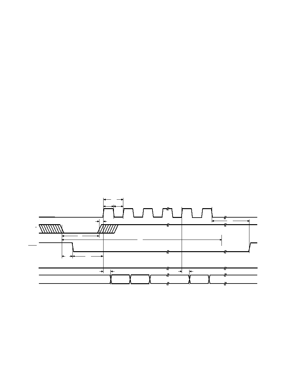
EXTERNAL DISCONTINUOUS CLOCK DATA READ
DURING CONVERSION NO SYNC OUTPUT
GENERATED
Figure 5 illustrates the method by which data from conversion
“n-1” can be read during conversion “n” while using a discon-
tinuous external clock, without the generation of a SYNC out-
put. After a conversion is initiated, indicated by
BUSY going
low, the result of the previous conversion can be read while
CS
is low and R/
C is high. In this mode CS can be tied low. The
MSB will be valid on the 1st falling edge and the 2nd rising
edge of DATACLK. The LSB will be valid on the 16th falling
edge and the 17th rising edge of DATACLK. A minimum of 16
clock pulses are required for DATACLK if the receiving device
will be latching data on the falling edge of DATACLK. A mini-
mum of 17 clock pulses are required for DATACLK if the
receiving device will be latching data on the rising edge of
DATACLK. Approximately 40 ns after the 17th rising edge of
DATACLK (if provided) the DATA output pin will reflect the
state of the TAG input pin during the first rising edge of
DATACLK.
For both the AD977 and the AD977A the data should be
clocked out during the first half of
BUSY so not to degrade
conversion performance. For the AD977 this requires use of a
4.8 MHz DATACLK or greater with data being read out as
soon as the conversion process begins. For the AD977A it
requires use of a 10 MHz DATACLK or greater.
It is not recommended that data be shifted through the TAG
input in this mode as it will certainly result in clocking of data
during the second half of the conversion.
EXTERNAL DISCONTINUOUS CLOCK DATA READ
AFTER CONVERSION WITH SYNC OUTPUT GENERATED
Figure 6 illustrates the method by which data from conversion
“n” can be read after the conversion is complete using a discon-
tinuous external clock, with the generation of a SYNC output.
What permits the generation of a SYNC output is a transition of
DATACLK while either
CS is high or while both CS and R/C
are low. After a conversion is complete, indicated by
BUSY
returning high, the result of that conversion can be read while
CS is Low and R/C is high. In this mode CS can be tied low. In
Figure 6 clock pulse #0 is used to enable the generation of a
SYNC pulse. The SYNC pulse is actually clocked out approxi-
mately 40 ns after the rising edge of clock pulse #1. The SYNC
pulse will be valid on the falling edge of clock pulse #1 and the
rising edge of clock pulse #2. The MSB will be valid on the
falling edge of clock pulse #2 and the rising edge of clock pulse
#3. The LSB will be valid on the falling edge of clock pulse #17
and the rising edge of clock pulse #18. Approximately 40 ns
after the rising edge of clock pulse #18 the DATA output pin
will reflect the state of the TAG input pin during the rising edge
of clock pulse #2. The advantage of this method of reading data
is that it is not being clocked out during a conversion and there-
fore conversion performance is not degraded.
When reading data after the conversion is complete, with the
highest frequency permitted for DATACLK (15.15 MHz),
and with the AD977A, the maximum possible throughput is
approximately 195 kHz and not the rated 200 kHz.
For details on use of the TAG input with this mode see the Use
of the TAG Input section.
R/C
BUSY
EXT
DATACLK
t13
t15
BIT 15
(MSB)
BIT 14
12
DATA
SYNC
t14
t12
015
16
t22
BIT 0
(LSB)
t18
t1
t21
t2
t18
t20
Figure 5. Conversion and Read Timing for Reading Previous Conversion Results During A Conversion Using External
Discontinuous Data Clock (EXT/
INT Set to Logic High, CS Set to Logic Low)
相关PDF资料 |
PDF描述 |
|---|---|
| VE-2NY-IU-F1 | CONVERTER MOD DC/DC 3.3V 132W |
| LTC2221CUP#TRPBF | IC ADC 12-BIT 135MSPS 64-QFN |
| VI-263-MX-S | CONVERTER MOD DC/DC 24V 75W |
| VE-2NX-IX-B1 | CONVERTER MOD DC/DC 5.2V 75W |
| IDT72V205L15TFI | IC FIFO SYNC 16KX9 15NS 64QFP |
相关代理商/技术参数 |
参数描述 |
|---|---|
| AD977ABRZ | 功能描述:IC ADC 16BIT 200KSPS 20-SOIC RoHS:是 类别:集成电路 (IC) >> 数据采集 - 模数转换器 系列:- 标准包装:1 系列:microPOWER™ 位数:8 采样率(每秒):1M 数据接口:串行,SPI? 转换器数目:1 功率耗散(最大):- 电压电源:模拟和数字 工作温度:-40°C ~ 125°C 安装类型:表面贴装 封装/外壳:24-VFQFN 裸露焊盘 供应商设备封装:24-VQFN 裸露焊盘(4x4) 包装:Digi-Reel® 输入数目和类型:8 个单端,单极 产品目录页面:892 (CN2011-ZH PDF) 其它名称:296-25851-6 |
| AD977ACN | 制造商:Analog Devices 功能描述:ADC Single SAR 200ksps 16-bit Serial 20-Pin PDIP N 制造商:Rochester Electronics LLC 功能描述:200 KSPS 16-BIT ADC - Bulk |
| AD977ACNZ | 功能描述:IC ADC 16BIT 200KSPS 20DIP RoHS:是 类别:集成电路 (IC) >> 数据采集 - 模数转换器 系列:- 产品培训模块:Lead (SnPb) Finish for COTS Obsolescence Mitigation Program 标准包装:2,500 系列:- 位数:12 采样率(每秒):3M 数据接口:- 转换器数目:- 功率耗散(最大):- 电压电源:- 工作温度:- 安装类型:表面贴装 封装/外壳:SOT-23-6 供应商设备封装:SOT-23-6 包装:带卷 (TR) 输入数目和类型:- |
| AD977ACR | 功能描述:IC ADC 16BIT 200KSPS 20-SOIC RoHS:否 类别:集成电路 (IC) >> 数据采集 - 模数转换器 系列:- 产品培训模块:Lead (SnPb) Finish for COTS Obsolescence Mitigation Program 标准包装:2,500 系列:- 位数:12 采样率(每秒):3M 数据接口:- 转换器数目:- 功率耗散(最大):- 电压电源:- 工作温度:- 安装类型:表面贴装 封装/外壳:SOT-23-6 供应商设备封装:SOT-23-6 包装:带卷 (TR) 输入数目和类型:- |
| AD977ACRS | 制造商:Analog Devices 功能描述:ADC Single SAR 200ksps 16-bit Serial 28-Pin SSOP |
发布紧急采购,3分钟左右您将得到回复。