- 您现在的位置:买卖IC网 > PDF目录17062 > AD9786-EBZ (Analog Devices Inc)BOARD EVALUATION FOR AD9786 PDF资料下载
参数资料
| 型号: | AD9786-EBZ |
| 厂商: | Analog Devices Inc |
| 文件页数: | 22/56页 |
| 文件大小: | 0K |
| 描述: | BOARD EVALUATION FOR AD9786 |
| 产品培训模块: | DAC Architectures |
| 标准包装: | 1 |
| 系列: | TxDAC+® |
| DAC 的数量: | 1 |
| 位数: | 16 |
| 采样率(每秒): | 500M |
| 数据接口: | 并联 |
| DAC 型: | 电流 |
| 工作温度: | -40°C ~ 85°C |
| 已供物品: | 板,CD |
| 已用 IC / 零件: | AD9786 |
第1页第2页第3页第4页第5页第6页第7页第8页第9页第10页第11页第12页第13页第14页第15页第16页第17页第18页第19页第20页第21页当前第22页第23页第24页第25页第26页第27页第28页第29页第30页第31页第32页第33页第34页第35页第36页第37页第38页第39页第40页第41页第42页第43页第44页第45页第46页第47页第48页第49页第50页第51页第52页第53页第54页第55页第56页
AD9786
Rev. B | Page 29 of 56
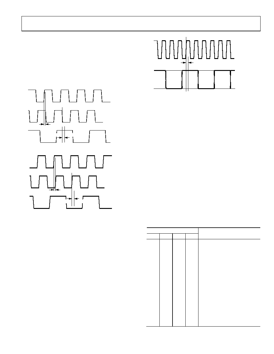
Low Setup/Hold Mode
(DATACLK Input, Data Recovery Off)
Some applications might require that digital input data be
synchronized with the DATACLK input, rather than DACCLK.
For these applications, the AD9786 can be programmed for low
setup/hold mode by entering the values in Table 26 into the SPI
registers. With data recovery off and the MODSYNC bit set to
Logic 1, the AD9786 latches data in upon the rising or falling
edge of DATACLK input, depending on the state of DCLKPOL.
03152-051
tHT = 0.0ns MIN
tS = –1.1ns MIN
tH = 2.8ns MIN
DACCLKIN
DATACLKIN
DATA
tST = 3.0ns MIN
Figure 51. Low Setup and Hold Mode Timing, 1× Interpolation, DCLKPOL = 0
03152-052
DACCLKIN
DATACLKIN
DATA
tS = –1.8ns MIN
tH = 3.1ns MIN
tHT = 1.0ns MIN
tST = 2.0ns MIN
Figure 52. Low Setup and Hold Mode Timing, 1× Interpolation, DCLKPOL = 1
External Sync Mode
In the external sync mode, the DATACLK is programmed as an
input but is not used. Applying a DATACLK input while in this
mode has no effect. The digital input data is synchronized solely
to the DACCLK input. With 1× interpolation, the data input is
latched upon every rising edge of DACCLK. The challenge is
that the user has no way of knowing exactly which edge is the
latching edge when the interpolating filters are in use. In 2×, 4×,
and 8× interpolation modes, the latching edge of DACCLK is
every 2nd, 4th, or 8th edge, respectively.
With the 2 ns keep-out window, shown in Figure 53, there is a
strong possibility of violating setup and hold times, especially at
high speeds. It is recommended that users sense the DAC output
noise floor for setup and hold violations. If setup and hold is violated,
DCLKPOL can be switched. The effect of switching the state of
DCLKPOL is that the latching edge is moved by one, two, or four
DACCLK cycles if the AD9786 is in 2×, 4×, or 8× interpolation
modes, respectively. Note that in this mode, the DATAADJ bits
have no effect.
03152-053
tS = –300ps MIN
tH = 2.9ns MIN
DACCLKIN
DATA
Figure 53. External Sync Mode with 2× Interpolation
Note that when using the AD9786 in external sync mode with
1× interpolation, that functionality is identical to master mode,
except that DATACLK out is not available. That is, with
DATACLKPOL = 0, data is latched on the falling edge of DACCLK,
and with DATACLKPOL = 1, data is latched on the rising edge
of DACCLK.
DATAADJUST Synchronization
When designing the digital interface for high speed DACs, care
must be taken to ensure that the DAC input data meets setup
and hold requirements. Often, compensation must be used in
the clock delay path to the digital engine driving the DAC. The
AD9786 has the on-chip capability to vary the latching edge of
DACCLK. With the interpolation function enabled, this allows
the user the choice of multiple edges upon which to latch the
data. For instance, if the AD9786 is using 8× interpolation, the
user can latch from one of eight edges before the rising edge of
DATACLK, or seven edges after this rising edge. The specific
edge upon which data is latched is controlled by SPI Register
0x05, Bits 7:4. Table 27 shows the relationship of the latching
edge of DACCLK and DATACLK with the various settings of
the DATAADJ bits.
Table 27. DATAADJ Values for Latching Edge Sync
SPI Register 0x05
Bit 7
Bit 6
Bit 5
Bit 4
Latching Edge Write DATACLK
0
1
+1
0
1
0
+2
0
1
+3
0
1
0
+4
0
1
0
1
+5
0
1
0
+6
0
1
+7
1
0
–8
1
0
1
–7
1
0
1
0
–6
1
0
1
–5
1
0
–4
1
0
1
–3
1
0
–2
1
–1
相关PDF资料 |
PDF描述 |
|---|---|
| MIC2099-1YMT TR | IC DISTRIBUTION SWITCH |
| RCA10DRMI-S288 | CONN EDGECARD 20POS .125 EXTEND |
| HBM11DSEN-S243 | CONN EDGECARD 22POS .156 EYELET |
| AD9772A-EBZ | BOARD EVAL FOR AD9772A |
| ECE-V1VA101UP | CAP ALUM 100UF 35V 20% SMD |
相关代理商/技术参数 |
参数描述 |
|---|---|
| AD9786XSV | 制造商:Analog Devices 功能描述:- Bulk |
| AD9787 | 制造商:AD 制造商全称:Analog Devices 功能描述:Dual 12-/14-/16-Bit 800 MSPS DAC with Low Power 32-Bit Complex NCO |
| AD9787BSVZ | 功能描述:IC DAC 14BIT 800MSPS 100TQFP RoHS:是 类别:集成电路 (IC) >> 数据采集 - 数模转换器 系列:TxDAC® 标准包装:1 系列:- 设置时间:4.5µs 位数:12 数据接口:串行,SPI? 转换器数目:1 电压电源:单电源 功率耗散(最大):- 工作温度:-40°C ~ 125°C 安装类型:表面贴装 封装/外壳:8-SOIC(0.154",3.90mm 宽) 供应商设备封装:8-SOICN 包装:剪切带 (CT) 输出数目和类型:1 电压,单极;1 电压,双极 采样率(每秒):* 其它名称:MCP4921T-E/SNCTMCP4921T-E/SNRCTMCP4921T-E/SNRCT-ND |
| AD9787BSVZRL | 功能描述:IC DAC 14BIT 800MSPS 100TQFP RoHS:是 类别:集成电路 (IC) >> 数据采集 - 数模转换器 系列:TxDAC® 产品培训模块:Data Converter Fundamentals DAC Architectures 标准包装:750 系列:- 设置时间:7µs 位数:16 数据接口:并联 转换器数目:1 电压电源:双 ± 功率耗散(最大):100mW 工作温度:0°C ~ 70°C 安装类型:表面贴装 封装/外壳:28-LCC(J 形引线) 供应商设备封装:28-PLCC(11.51x11.51) 包装:带卷 (TR) 输出数目和类型:1 电压,单极;1 电压,双极 采样率(每秒):143k |
| AD9787-DPG2-EBZ | 功能描述:BOARD EVALUATION FOR AD9787 RoHS:是 类别:编程器,开发系统 >> 评估板 - 数模转换器 (DAC) 系列:* 产品培训模块:Lead (SnPb) Finish for COTS Obsolescence Mitigation Program 标准包装:1 系列:- DAC 的数量:4 位数:12 采样率(每秒):- 数据接口:串行,SPI? 设置时间:3µs DAC 型:电流/电压 工作温度:-40°C ~ 85°C 已供物品:板 已用 IC / 零件:MAX5581 |
发布紧急采购,3分钟左右您将得到回复。