- 您现在的位置:买卖IC网 > PDF目录17062 > AD9786-EBZ (Analog Devices Inc)BOARD EVALUATION FOR AD9786 PDF资料下载
参数资料
| 型号: | AD9786-EBZ |
| 厂商: | Analog Devices Inc |
| 文件页数: | 37/56页 |
| 文件大小: | 0K |
| 描述: | BOARD EVALUATION FOR AD9786 |
| 产品培训模块: | DAC Architectures |
| 标准包装: | 1 |
| 系列: | TxDAC+® |
| DAC 的数量: | 1 |
| 位数: | 16 |
| 采样率(每秒): | 500M |
| 数据接口: | 并联 |
| DAC 型: | 电流 |
| 工作温度: | -40°C ~ 85°C |
| 已供物品: | 板,CD |
| 已用 IC / 零件: | AD9786 |
第1页第2页第3页第4页第5页第6页第7页第8页第9页第10页第11页第12页第13页第14页第15页第16页第17页第18页第19页第20页第21页第22页第23页第24页第25页第26页第27页第28页第29页第30页第31页第32页第33页第34页第35页第36页当前第37页第38页第39页第40页第41页第42页第43页第44页第45页第46页第47页第48页第49页第50页第51页第52页第53页第54页第55页第56页

AD9786
Rev. B | Page 42 of 56
Master/Slave, Modulator/DATACLK Master Modes
In applications where two or more AD9786s are used to synthe-
size several digital data paths, it might be necessary to ensure
that the digital inputs to each device are latched synchronously.
In complex data processing applications, digital modulator phase
alignment might be required between two AD9786s. To allow
data synchronization and phase alignment, only one AD9786
should be configured as a master device, providing a reference
clock for another slave-configured AD9786.
With synchronization enabled, a reference clock signal is
generated on the DATACLK pin of the master. The DATACLK
pins on the slave devices act as inputs for the reference clock
generated by the master. The DATACLK pin on the master and
all slaves must be directly connected. All master and slave devices
must have the same clock source connected to their respective
CLK+/CLK– pins.
When configured as a master, the reference clock generated can
take one of two forms. In modulator master mode, the reference
clock is a square wave with a period equal to 16 cycles of the
DAC update clock. Internal to the AD9786 is a 16-state, finite
state machine, running at the DAC update rate. This state machine
generates all internal and external synchronization clocks and
modulator phasings. The rising edge of the master reference clock
is time aligned to state zero of the internal state machine. Slave
devices use the master reference clock to synchronize data latching
and align modulator phase by aligning state zero of the local
state machine to the master.
The second master mode, DATACLK master mode, generates a
reference clock that is at the channel data rate. In this mode, the
slave devices align their internal channel data rate clock to the
master. If modulator phase alignment is needed, a concurrent
serial write to all slave devices is necessary. To achieve this, the
CSB pin on all slaves must be connected together, and a group
serial write to the MODADJ register bits must be performed.
Following a successful serial write, the modulator coefficient
alignment is updated upon the next rising edge of the internal
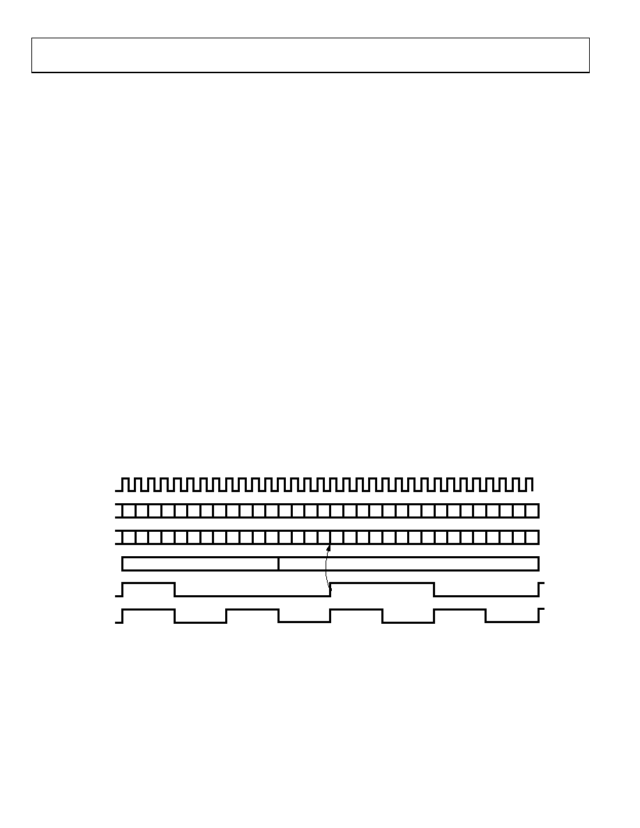
state machine (see Figure 81). Modulator master mode does not
need a concurrent serial write, because slaves lock to the master
phase automatically.
In a slave device, the local channel data rate clock and the
digital modulator clock are created from the internal state
machine. The local channel data rate clock is used by the slave
to latch digital input data. At high data rates, the delay inherent
in the signal path from master to slave can cause the slave to lag
the master when acquiring synchronization. To accommodate
for this, an integer number of the DAC update clock cycles can
be programmed into the slave device as an offset. The value in
DATAADJ allows the local channel data rate clock in the slave
device to advance by up to eight cycles of the DAC clock, or to
be delayed by up to seven cycles (see Figure 82).
The digital modulator coefficients are updated at the DAC clock
rate and decoded in sequential order from the state machine
according to Figure 83. The MODADJ bits can be used to align
a different coefficient to the finite state machine’s zero state, as
shown in Figure 84.
DAC
CLOCK
STATE
MACHINE
STATE MACHINE
CHANNEL DATA
CYCLE CLOCK
RATE CLOCK
MODULATOR
COEFFICIENT
MODADJ
000
10
–1
010
–1
010
–1
010
–1
0
–1
0
10
–1
01
0
–1
0
1
0
–1
01
0
01
2345
6789
10
11
12
13
14
15
01
23456
789
10
11
12
13
14
15
03152-081
Figure 81. Synchronous Serial Modulator Phase Alignment
相关PDF资料 |
PDF描述 |
|---|---|
| MIC2099-1YMT TR | IC DISTRIBUTION SWITCH |
| RCA10DRMI-S288 | CONN EDGECARD 20POS .125 EXTEND |
| HBM11DSEN-S243 | CONN EDGECARD 22POS .156 EYELET |
| AD9772A-EBZ | BOARD EVAL FOR AD9772A |
| ECE-V1VA101UP | CAP ALUM 100UF 35V 20% SMD |
相关代理商/技术参数 |
参数描述 |
|---|---|
| AD9786XSV | 制造商:Analog Devices 功能描述:- Bulk |
| AD9787 | 制造商:AD 制造商全称:Analog Devices 功能描述:Dual 12-/14-/16-Bit 800 MSPS DAC with Low Power 32-Bit Complex NCO |
| AD9787BSVZ | 功能描述:IC DAC 14BIT 800MSPS 100TQFP RoHS:是 类别:集成电路 (IC) >> 数据采集 - 数模转换器 系列:TxDAC® 标准包装:1 系列:- 设置时间:4.5µs 位数:12 数据接口:串行,SPI? 转换器数目:1 电压电源:单电源 功率耗散(最大):- 工作温度:-40°C ~ 125°C 安装类型:表面贴装 封装/外壳:8-SOIC(0.154",3.90mm 宽) 供应商设备封装:8-SOICN 包装:剪切带 (CT) 输出数目和类型:1 电压,单极;1 电压,双极 采样率(每秒):* 其它名称:MCP4921T-E/SNCTMCP4921T-E/SNRCTMCP4921T-E/SNRCT-ND |
| AD9787BSVZRL | 功能描述:IC DAC 14BIT 800MSPS 100TQFP RoHS:是 类别:集成电路 (IC) >> 数据采集 - 数模转换器 系列:TxDAC® 产品培训模块:Data Converter Fundamentals DAC Architectures 标准包装:750 系列:- 设置时间:7µs 位数:16 数据接口:并联 转换器数目:1 电压电源:双 ± 功率耗散(最大):100mW 工作温度:0°C ~ 70°C 安装类型:表面贴装 封装/外壳:28-LCC(J 形引线) 供应商设备封装:28-PLCC(11.51x11.51) 包装:带卷 (TR) 输出数目和类型:1 电压,单极;1 电压,双极 采样率(每秒):143k |
| AD9787-DPG2-EBZ | 功能描述:BOARD EVALUATION FOR AD9787 RoHS:是 类别:编程器,开发系统 >> 评估板 - 数模转换器 (DAC) 系列:* 产品培训模块:Lead (SnPb) Finish for COTS Obsolescence Mitigation Program 标准包装:1 系列:- DAC 的数量:4 位数:12 采样率(每秒):- 数据接口:串行,SPI? 设置时间:3µs DAC 型:电流/电压 工作温度:-40°C ~ 85°C 已供物品:板 已用 IC / 零件:MAX5581 |
发布紧急采购,3分钟左右您将得到回复。