- 您现在的位置:买卖IC网 > PDF目录378276 > AD9878 (Analog Devices, Inc.) Mixed-Signal Front End for Broadband Applications PDF资料下载
参数资料
| 型号: | AD9878 |
| 厂商: | Analog Devices, Inc. |
| 元件分类: | 开关 |
| 英文描述: | Mixed-Signal Front End for Broadband Applications |
| 中文描述: | 混合信号的宽带应用前端 |
| 文件页数: | 28/36页 |
| 文件大小: | 749K |
| 代理商: | AD9878 |
第1页第2页第3页第4页第5页第6页第7页第8页第9页第10页第11页第12页第13页第14页第15页第16页第17页第18页第19页第20页第21页第22页第23页第24页第25页第26页第27页当前第28页第29页第30页第31页第32页第33页第34页第35页第36页
AD9878
Driving the Input
The IF ADCs have differential switched capacitor sample-and-
hold amplifier (SHA) inputs. The nominal differential input
impedance is 4.0 k||3 pF. This impedance can be used as the
effective termination impedance when calculating filter transfer
characteristics and voltage signal attenuation from nonzero source
impedances. For best performance, additional requirements must
be met by the signal source. The SHA has input capacitors that
must be recharged each time the input is sampled. This results in
a dynamic input current at the device input, and demands that
the source has low (<50 ) output impedance at frequencies up
to the ADC sampling frequency. Also, the source must have
settling of better than 0.1% in less than half the ADC clock period.
Rev. A | Page 28 of 36
Another consideration for getting the best performance from the
ADC inputs is the dc biasing of the input signal. Ideally, the signal
should be biased to a dc level equal to the midpoint of the ADC
reference voltages, REFT12 and REFB12. Nominally, this level is
1.2 V. When ac-coupled, the ADC inputs self-bias to this voltage
and require no additional input circuitry. Figure 35 illustrates a
recommended circuit that eases the burden on the signal source
by isolating its output from the ADC input. The 33 series
termination resistors isolate the amplifier outputs from any
capacitive load, which typically improves settling time. The series
capacitors provide ac signal coupling, which ensures that the
ADC inputs operate at the optimal dc-bias voltage. The shunt
capacitor sources the dynamic currents required to charge the
SHA input capacitors, removing this requirement from the ADC
buffer. The values of C
C
and C
S
should be calculated to
determine the correct HPF and LPF corner frequencies.
AIN+
AIN–
33
C
C
C
S
C
C
V
S
33
0
Figure 35. Simple ADC Drive Configuration
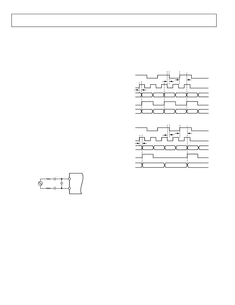
Receive Timing
The AD9878 sends multiplexed data to the IF10 and IF12 outputs
upon every rising edge of MCLK. RxSYNC frames the start of
each IF10 data symbol. The 10-bit and 12-bit ADCs are read
completely upon every second MCLK cycle. RxSYNC is high
for every second 10-bit ADC data if the 10-bit ADC is not in
power-down mode. The Rx timing diagram is shown in Figure 36.
t
OD
t
EE
t
MD
REFCLK
MCLK
IF10 DATA
IF10[9:5] IF10[4:0] IF10[9:5] IF10[4:0]
M/N = 2
IF10[9:5] IF10[4:0]
IF12A
IF12B
IF12B
IF12B
IF12A
IF12B
RxSYNC
IF12 DATA
Rx PORT TIMING (DEFAULT MODE: MUXED IF12 ADC DATA)
M/N = 2
REFCLK
IF12A OR IF12B
IF12A OR IF12B
IF10[9:5]
IF10[4:0]
IF10[9:5]
IF10[4:0]
IF10[9:5]
IF10[4:0]
IF12A OR IF12B
MCLK
IF10 DATA
RxSYNC
IF DATA
t
MD
t
EE
t
OD
Rx PORT TIMING (OUTPUT DATA FROM ONLY ONE IF12 ADC)
0
Figure 36. Rx Port Timing
相关PDF资料 |
PDF描述 |
|---|---|
| AD9878-EB | Mixed-Signal Front End for Broadband Applications |
| AD9878BST | Mixed-Signal Front End for Broadband Applications |
| AD9878BSTZ | Mixed-Signal Front End for Broadband Applications |
| ADAV801 | Audio Codec for Recordable DVD |
| ADAV801ASTZ | Audio Codec for Recordable DVD |
相关代理商/技术参数 |
参数描述 |
|---|---|
| AD9878BST | 制造商:Analog Devices 功能描述:Mixed Signal Front End 100-Pin LQFP |
| AD9878BSTRL | 制造商:Analog Devices 功能描述:Mixed Signal Front End 100-Pin LQFP T/R 制造商:Analog Devices 功能描述:MIXED SGNL FRONT END 100LQFP - Tape and Reel |
| AD9878BSTZ | 功能描述:IC FRONT-END MIXED-SGNL 100-LQFP RoHS:是 类别:集成电路 (IC) >> 数据采集 - 模拟前端 (AFE) 系列:- 产品培训模块:Lead (SnPb) Finish for COTS Obsolescence Mitigation Program 标准包装:2,500 系列:- 位数:- 通道数:2 功率(瓦特):- 电压 - 电源,模拟:3 V ~ 3.6 V 电压 - 电源,数字:3 V ~ 3.6 V 封装/外壳:32-VFQFN 裸露焊盘 供应商设备封装:32-QFN(5x5) 包装:带卷 (TR) |
| AD9878-EB | 制造商:Analog Devices 功能描述:EVAL KIT FOR MIXED-SGNL FRONT END FOR BROADBAND APPLICATIONS - Bulk |
| AD9879 | 制造商:AD 制造商全称:Analog Devices 功能描述:Mixed-Signal Front End Set-Top Box, Cable Modem |
发布紧急采购,3分钟左右您将得到回复。