- 您现在的位置:买卖IC网 > PDF目录10978 > AD9911BCPZ (Analog Devices Inc)IC DDS 500MSPS DAC 10BIT 56LFCSP PDF资料下载
参数资料
| 型号: | AD9911BCPZ |
| 厂商: | Analog Devices Inc |
| 文件页数: | 13/44页 |
| 文件大小: | 0K |
| 描述: | IC DDS 500MSPS DAC 10BIT 56LFCSP |
| 产品培训模块: | Direct Digital Synthesis Tutorial Series (1 of 7): Introduction Direct Digital Synthesizer Tutorial Series (7 of 7): DDS in Action Direct Digital Synthesis Tutorial Series (3 of 7): Angle to Amplitude Converter Direct Digital Synthesis Tutorial Series (6 of 7): SINC Envelope Correction Direct Digital Synthesis Tutorial Series (4 of 7): Digital-to-Analog Converter Direct Digital Synthesis Tutorial Series (2 of 7): The Accumulator |
| 标准包装: | 1 |
| 分辨率(位): | 10 b |
| 主 fclk: | 500MHz |
| 调节字宽(位): | 32 b |
| 电源电压: | 1.71 V ~ 1.96 V |
| 工作温度: | -40°C ~ 85°C |
| 安装类型: | 表面贴装 |
| 封装/外壳: | 56-VFQFN 裸露焊盘,CSP |
| 供应商设备封装: | 56-LFCSP-VQ(8x8) |
| 包装: | 托盘 |
| 配用: | AD9911/PCBZ-ND - BOARD EVAL FOR AD9911 |
第1页第2页第3页第4页第5页第6页第7页第8页第9页第10页第11页第12页当前第13页第14页第15页第16页第17页第18页第19页第20页第21页第22页第23页第24页第25页第26页第27页第28页第29页第30页第31页第32页第33页第34页第35页第36页第37页第38页第39页第40页第41页第42页第43页第44页
AD9911
Rev. 0 | Page 20 of 44
DATA
ALIGN
10-BIT DAC
DAC 1
COS(X)
DDS CORE 1
MUX
0
CFR <18:16>
10
COS(X)
DDS CORE 0
COS(X)
DDS CORE 2
COS(X)
DDS CORE 3
10
3
10
3
05
78
5-
03
5
DATA
ALIGN
DATA
ALIGN
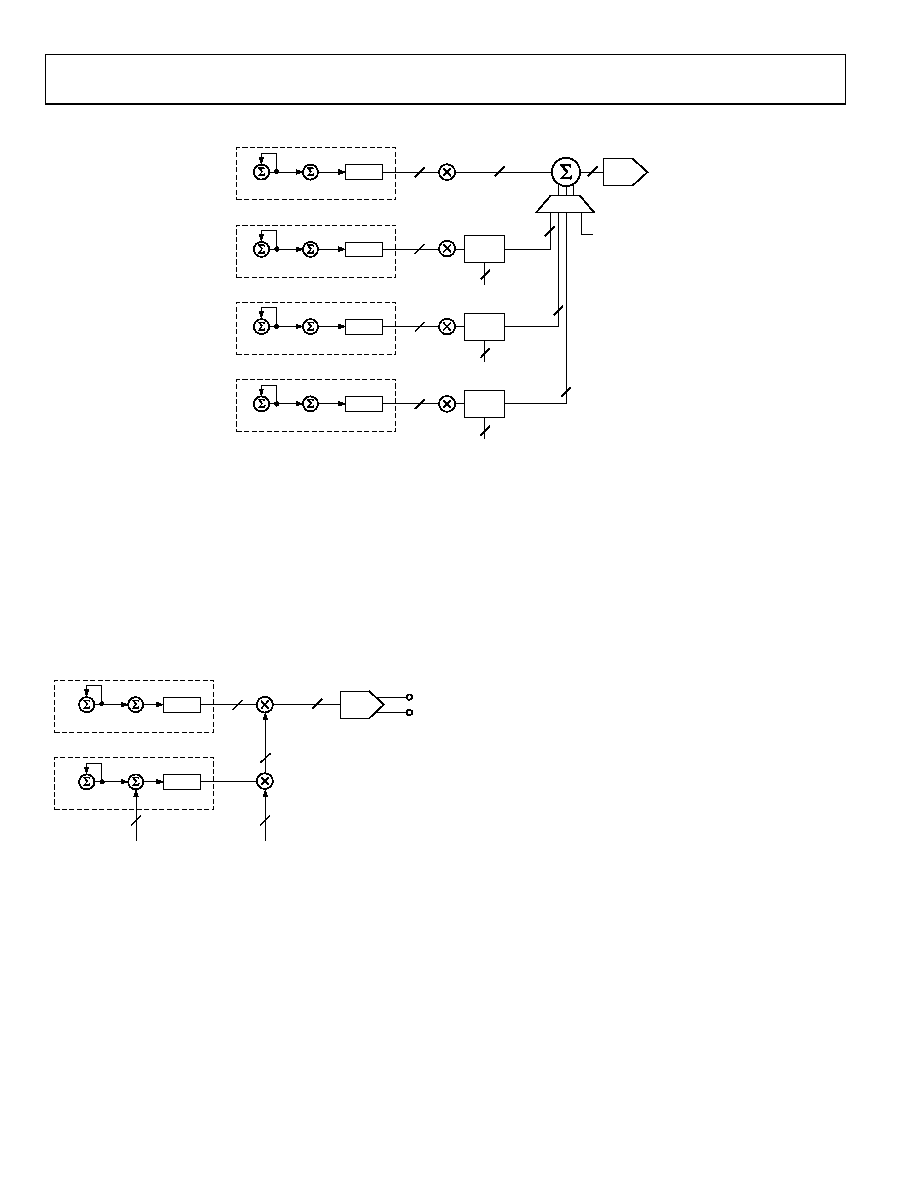
Figure 36. SpurKiller/Multitone Mode Configuration
TEST-TONE MODE
Test-tone mode enables sinusoidal amplitude modulation of the
carrier (CH1). Setting Bit 2 in Register 0x01 enables test-tone
mode. Auxiliary CH2 and CH3 should both be disabled using
the channel enable bits (CSR Bit <7>). The frequency of
modulation is set using the frequency tuning word
(Register 0x04 Bits <31:0>) of auxiliary CH0. Auxiliary CH0
output scalar (Register 0x06 Bits <0:9>) sets the magnitude of
the modulating signal. See Figure 37 for a diagram of the test-
tone mode configuration.
DAC 1
COS(X)
DDS CORE 1
10
14
10
COS(X)
DDS CORE 0
PHASE OFFSET
AMPLITUDE
05
78
5-
0
36
Figure 37. Test-Tone Mode Configuration
REFERENCE CLOCK MODES
The AD9911 supports several methods for generating the
internal system clock. An on-chip oscillator circuit is available
for initiating the low frequency reference signal by connecting
a crystal to the clock input pins. The system clock can also be
generated using the internal, PLL-based reference clock
multiplier, allowing the part to operate with a low frequency
clock source while still providing a high sample rate for the
DDS and DAC. For best phase noise performance, a clean,
stable clock with a high slew rate is required.
Enabling the PLL allows multiplication of the reference clock
frequency from 4× to 20×, in integer steps. The PLL multiplica-
tion value is 5-bits located in the Function Register 1 (FR1) Bits
<22:18>. For further information, refer to the Register Map
section.
When FR1 <22:18> is programmed with values ranging from 4 to
20 (decimal), the clock multiplier is enabled. The integer value in
the register represents the multiplication factor. The system clock
rate with the clock multiplier enabled is equal to the reference clock
rate times the multiplication factor. If FR1 <22:18> is programmed
with a value less than 4 or greater than 20, the clock multiplier is
disabled. Note that the output frequency of the PLL has a restricted
frequency range. There is a VCO gain bit that must be set
appropriately. The VCO gain bit (FR1<23>) defines two ranges
(low/high) of frequency output. See the Register Map section for
configuration directions and defaults.
The charge pump current in the PLL defaults to 75 μA, which
typically produces the best phase noise characteristics.
Increasing charge pump current typically degrades phase noise,
but decreases the lock time and alters the loop bandwidth. The
charge pump control bits (FR1 <17:16>) function is described
in the Register Map section.
To enable the on-chip oscillator for crystal operation, drive
CLK_MODE_SEL (Pin 24) high. The CLKMODESEL pin is
considered an analog input, operating on 1.8 V logic. With the
on-chip oscillator enabled, connection of an external crystal to
the REF_CLK and REF_CLKB inputs is made producing a low
frequency reference clock. The crystal frequency must be in the
range of 20 MHz to 30 MHz. summarizes the clock mode
options. See the Register Maps section for more details.
相关PDF资料 |
PDF描述 |
|---|---|
| VE-B11-IY-F4 | CONVERTER MOD DC/DC 12V 50W |
| VE-B11-IY-F1 | CONVERTER MOD DC/DC 12V 50W |
| VE-2WZ-IY-F4 | CONVERTER MOD DC/DC 2V 20W |
| VE-2WZ-IY-F1 | CONVERTER MOD DC/DC 2V 20W |
| VE-2WZ-IX-F2 | CONVERTER MOD DC/DC 2V 30W |
相关代理商/技术参数 |
参数描述 |
|---|---|
| AD9911BCPZ-REEL7 | 功能描述:IC DDS 500MSPS DAC 10BIT 56LFCSP RoHS:是 类别:集成电路 (IC) >> 接口 - 直接数字合成 (DDS) 系列:- 产品变化通告:Product Discontinuance 27/Oct/2011 标准包装:2,500 系列:- 分辨率(位):10 b 主 fclk:25MHz 调节字宽(位):32 b 电源电压:2.97 V ~ 5.5 V 工作温度:-40°C ~ 85°C 安装类型:表面贴装 封装/外壳:16-TSSOP(0.173",4.40mm 宽) 供应商设备封装:16-TSSOP 包装:带卷 (TR) |
| AD9912 | 制造商:AD 制造商全称:Analog Devices 功能描述:1 GSPS Direct Digital Synthesizer w/ 14-bit DAC |
| AD9912/PCBZ | 制造商:Analog Devices 功能描述:Evaluation Kit For 1 GSPS Direct Digital Synthesizer W/ 14-Bit DAC 制造商:Analog Devices 功能描述:EVAL KIT FOR 1 GSPS DIRECT DGTL SYNTHESIZER W/ 14BIT DAC - Bulk 制造商:Analog Devices 功能描述:EVALUATION BOARD AD9912 1GSPS DDS |
| AD9912A/PCBZ | 功能描述:BOARD EVALUATION FOR AD9912 RoHS:是 类别:编程器,开发系统 >> 评估演示板和套件 系列:- 标准包装:1 系列:PCI Express® (PCIe) 主要目的:接口,收发器,PCI Express 嵌入式:- 已用 IC / 零件:DS80PCI800 主要属性:- 次要属性:- 已供物品:板 |
| AD9912ABCPZ | 功能描述:IC DDS 1GSPS DAC 14BIT 64LFCSP RoHS:是 类别:集成电路 (IC) >> 接口 - 直接数字合成 (DDS) 系列:- 产品变化通告:Product Discontinuance 27/Oct/2011 标准包装:2,500 系列:- 分辨率(位):10 b 主 fclk:25MHz 调节字宽(位):32 b 电源电压:2.97 V ~ 5.5 V 工作温度:-40°C ~ 85°C 安装类型:表面贴装 封装/外壳:16-TSSOP(0.173",4.40mm 宽) 供应商设备封装:16-TSSOP 包装:带卷 (TR) |
发布紧急采购,3分钟左右您将得到回复。