- 您现在的位置:买卖IC网 > PDF目录1988 > AD9920ABBCZRL (Analog Devices Inc)IC PROCESSOR CCD 12BIT 105CSPBGA PDF资料下载
参数资料
| 型号: | AD9920ABBCZRL |
| 厂商: | Analog Devices Inc |
| 文件页数: | 2/112页 |
| 文件大小: | 0K |
| 描述: | IC PROCESSOR CCD 12BIT 105CSPBGA |
| 标准包装: | 2,000 |
| 位数: | 12 |
| 电压 - 电源,模拟: | 1.6 V ~ 2 V |
| 电压 - 电源,数字: | 1.6 V ~ 2 V |
| 封装/外壳: | 105-LFBGA,CSPBGA |
| 供应商设备封装: | 105-CSPBGA(8x8) |
| 包装: | 带卷 (TR) |
第1页当前第2页第3页第4页第5页第6页第7页第8页第9页第10页第11页第12页第13页第14页第15页第16页第17页第18页第19页第20页第21页第22页第23页第24页第25页第26页第27页第28页第29页第30页第31页第32页第33页第34页第35页第36页第37页第38页第39页第40页第41页第42页第43页第44页第45页第46页第47页第48页第49页第50页第51页第52页第53页第54页第55页第56页第57页第58页第59页第60页第61页第62页第63页第64页第65页第66页第67页第68页第69页第70页第71页第72页第73页第74页第75页第76页第77页第78页第79页第80页第81页第82页第83页第84页第85页第86页第87页第88页第89页第90页第91页第92页第93页第94页第95页第96页第97页第98页第99页第100页第101页第102页第103页第104页第105页第106页第107页第108页第109页第110页第111页第112页
AD9920A
Rev. B | Page 10 of 112
ABSOLUTE MAXIMUM RATINGS
Stresses above those listed under Absolute Maximum Ratings
may cause permanent damage to the device. This is a stress
rating only; functional operation of the device at these or any
other conditions above those indicated in the operational
section of this specification is not implied. Exposure to absolute
maximum rating conditions for extended periods may affect
device reliability.
Table 6.
Parameter
Rating
AVDD to AVSS
0.3 V to +2.2 V
TCVDD to TCVSS
0.3 V to +2.2 V
HVDD1, HVDD2 to HVSS1, HVSS2
0.3 V to +3.9 V
RGVDD to RGVSS
0.3 V to +3.9 V
DVDD to DVSS
0.3 V to +2.2 V
DRVDD to DRVSS/LDOVSS
0.3 V to +3.9 V
IOVDD to IOVSS
0.3 V to +3.9 V
VDVDD to VDVSS
0.3 V to +3.9 V
CLIVDD to TCVSS
0.3 V to +3.9 V
VH1, VH2 to VL1, VL2, VLL
0.3 V to +25.0 V
VH1, VH2 to VDVSS
0.3 V to +17.0 V
VL1, VL2 to VDVSS
17.0 V to +0.3 V
VM1, VM2 to VDVSS
6.0 V to +3.0 V
VLL to VDVSS
17.0 V to +0.3 V
VMM to VDVSS
VLL 0.3 V to VDVDD + 0.3 V
V1A to V16 to VDVSS
VLx 0.3 V to VHx + 0.3 V
RG and HL Outputs to RGVSS
0.3 V to RGVDD + 0.3 V
H1 to H8 Outputs to HVSSx
0.3 V to HVDDx + 0.3 V
VDR_EN, XSUBCNT, SRCTL, SRSW
to VDVSS
0.3 V to VDVDD + 0.3 V
Digital Outputs to IOVSS
0.3 V to IOVDD + 0.3 V
Digital Inputs to IOVSS
0.3 V to IOVDD + 0.3 V
SCK, SL, SDATA to DVSS
0.3 V to DVDD + 0.3 V
REFT, REFB, CCDIN to AVSS
0.3 V to AVDD + 0.3 V
Junction Temperature
150°C
Lead Temperature
(Soldering, 10 sec)
350°C
THERMAL RESISTANCE
θJA is specified for the worst-case conditions, that is, a device
soldered in a circuit board for surface-mount packages.
Table 7. Thermal Resistance
Package Type
θJA
Unit
CSP_BGA (BC-105-1)
40.3
°C/W
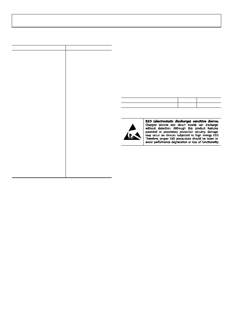
ESD CAUTION
相关PDF资料 |
PDF描述 |
|---|---|
| AD9978BCPZRL | IC PROCESSOR CCD 14BIT 40-LFCSP |
| ADADC71KD | IC ADC 16BIT HIGH RES 32-CDIP |
| ADADC80-Z-12 | IC ADC 12BIT INTEGRATED 32-CDIP |
| ADATE207BBPZ | IC TIMING FORMATTER QUAD 256BGA |
| ADC0804LCN | IC ADC 8-BIT 10KSPS 1LSB 20-DIP |
相关代理商/技术参数 |
参数描述 |
|---|---|
| AD9920BBCZ | 制造商:Analog Devices 功能描述: |
| AD9920BBCZRL | 制造商:Rochester Electronics LLC 功能描述: 制造商:Analog Devices 功能描述: |
| AD9921BBCZ | 制造商:Analog Devices 功能描述: |
| AD9921BBCZRL | 制造商:Analog Devices 功能描述: |
| AD9923A | 制造商:AD 制造商全称:Analog Devices 功能描述:CCD Signal Processor with V-Driver and Precision Timing⑩ Generator |
发布紧急采购,3分钟左右您将得到回复。