- 您现在的位置:买卖IC网 > PDF目录11659 > AD9949AKCPZRL (Analog Devices Inc)IC CCD SIGNAL PROCESSOR 40-LFCSP PDF资料下载
参数资料
| 型号: | AD9949AKCPZRL |
| 厂商: | Analog Devices Inc |
| 文件页数: | 16/36页 |
| 文件大小: | 0K |
| 描述: | IC CCD SIGNAL PROCESSOR 40-LFCSP |
| 标准包装: | 2,500 |
| 类型: | CCD 信号处理器,12 位 |
| 输入类型: | 逻辑 |
| 输出类型: | 逻辑 |
| 接口: | 3 线串口 |
| 安装类型: | 表面贴装 |
| 封装/外壳: | 40-VFQFN 裸露焊盘,CSP |
| 供应商设备封装: | 40-LFCSP |
| 包装: | 带卷 (TR) |
第1页第2页第3页第4页第5页第6页第7页第8页第9页第10页第11页第12页第13页第14页第15页当前第16页第17页第18页第19页第20页第21页第22页第23页第24页第25页第26页第27页第28页第29页第30页第31页第32页第33页第34页第35页第36页
AD9949
Rev. B | Page 23 of 36
GENERATING SPECIAL HBLK PATTERNS
Six toggle positions are available for HBLK. Normally, only two
of the toggle positions are used to generate the standard HBLK
interval. However, the additional toggle positions may be used
to generate special HBLK patterns, as shown in Figure 24. The
pattern in this example uses all six toggle positions to generate
two extra groups of pulses during the HBLK interval. By
changing the toggle positions, different patterns can be created.
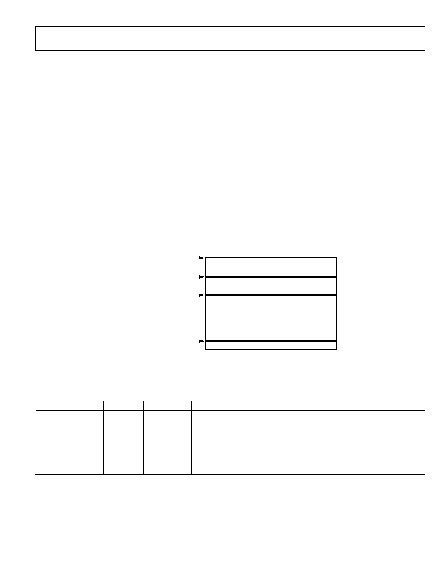
HORIZONTAL SEQUENCE CONTROL
The AD9949 uses sequence change positions (SCP) and
sequence pointers (SPTR) to organize the individual horizontal
sequences. Up to four SCPs are available to divide the readout
into four separate regions, as shown in Figure 25. The SCP0 is
always hard-coded to Line 0, and SCP1 to SCP3 are register
programmable. During each region bounded by the SCP, the
SPTR registers designate which sequence is used by each signal.
CLPOB, PBLK, and HBLK each have a separate set of SCPs. For
example, CLPOBSCP1 defines Region 0 for CLPOB, and in that
region any of the four individual CLPOB sequences may be
selected with the CLPOBSPTR register. The next SCP defines a
new region and in that region, each signal can be assigned to a
different individual sequence. The sequence control registers
are summarized in Table 20.
EXTERNAL HBLK SIGNAL
The AD9949 can also be used with an external HBLK signal.
Setting the HBLKDIR register (Address 0×40) to high disables
the internal HBLK signal generation. The polarity of the exter-
nal signal is specified using the HBLKPOL register, and the
masking polarity of H1 is specified using the HBLKMASK
register. Table 21 summarizes the register values when using an
external HBLK signal.
UP TO FOUR INDIVIDUAL HORIZONTAL CLAMP AND BLANKING REGIONS MAY BE
PROGRAMMED WITHIN A SINGLE FIELD, USING THE SEQUENCE CHANGE POSITIONS.
SEQUENCE CHANGE OF POSITION 1
SEQUENCE CHANGE OF POSITION 2
SEQUENCE CHANGE OF POSITION 3
SINGLE FIELD (1 VD INTERVAL)
CLAMP AND PBLK SEQUENCE REGION 0
SEQUENCE CHANGE OF POSITION 0
(V-COUNTER = 0)
CLAMP AND PBLK SEQUENCE REGION 3
CLAMP AND PBLK SEQUENCE REGION 2
CLAMP AND PBLK SEQUENCE REGION 1
03751-026
Figure 25. Clamp and Blanking Sequence Flexibility
Table 21. External HBLK Register Parameters
Register
Length
Range
Description
HBLKDIR
1b
High/Low
Specifies HBLK Internally Generated or Externally Supplied.
1 = External.
HBLKPOL
1b
High/Low
External HBLK Active Polarity.
0 = Active Low.
1 = Active High.
HBLKEXTMASK
1b
High/Low
External HBLK Masking Polarity.
0 = Mask H1 Low.
1 = Mask H1 High.
相关PDF资料 |
PDF描述 |
|---|---|
| 2081204-9 | CONN JACK SMA BULKHEAD RG405 |
| AD9949KCPZRL | IC CCD SIGNAL PROCESSOR 40-LFCSP |
| 2081204-7 | CONN JACK SMA BULKHEAD RG58 |
| 2081204-5 | CONN JACK SMA BULKHEAD RD316 |
| AD9948KCPZRL | IC CCD SIGNAL PROCESSOR 40-LFCSP |
相关代理商/技术参数 |
参数描述 |
|---|---|
| AD9949BCBZRL | 制造商:Analog Devices 功能描述: |
| AD9949KCP | 制造商:Analog Devices 功能描述:AFE Video 1ADC 12-Bit 3V 40-Pin LFCSP EP 制造商:Rochester Electronics LLC 功能描述:12 BIT 36 MSPS, 3 V ANALOG FRONT END - Bulk |
| AD9949KCPRL | 制造商:Analog Devices 功能描述:AFE Video 1ADC 12-Bit 3V 40-Pin LFCSP EP T/R 制造商:Rochester Electronics LLC 功能描述:12 BIT 36 MSPS, 3 V ANALOG FRONT END - Tape and Reel |
| AD9949KCPZ | 功能描述:IC CCD SIGNAL PROCESSOR 40-LFCSP RoHS:是 类别:集成电路 (IC) >> 接口 - 传感器和探测器接口 系列:- 其它有关文件:Automotive Product Guide 产品培训模块:Lead (SnPb) Finish for COTS Obsolescence Mitigation Program 标准包装:74 系列:- 类型:触控式传感器 输入类型:数字 输出类型:数字 接口:JTAG,串行 电流 - 电源:100µA 安装类型:表面贴装 封装/外壳:20-TSSOP(0.173",4.40mm 宽) 供应商设备封装:20-TSSOP 包装:管件 |
| AD9949KCPZRL | 功能描述:IC CCD SIGNAL PROCESSOR 40-LFCSP RoHS:是 类别:集成电路 (IC) >> 接口 - 传感器和探测器接口 系列:- 其它有关文件:Automotive Product Guide 产品培训模块:Lead (SnPb) Finish for COTS Obsolescence Mitigation Program 标准包装:74 系列:- 类型:触控式传感器 输入类型:数字 输出类型:数字 接口:JTAG,串行 电流 - 电源:100µA 安装类型:表面贴装 封装/外壳:20-TSSOP(0.173",4.40mm 宽) 供应商设备封装:20-TSSOP 包装:管件 |
发布紧急采购,3分钟左右您将得到回复。