- 您现在的位置:买卖IC网 > PDF目录11659 > AD9949AKCPZRL (Analog Devices Inc)IC CCD SIGNAL PROCESSOR 40-LFCSP PDF资料下载
参数资料
| 型号: | AD9949AKCPZRL |
| 厂商: | Analog Devices Inc |
| 文件页数: | 25/36页 |
| 文件大小: | 0K |
| 描述: | IC CCD SIGNAL PROCESSOR 40-LFCSP |
| 标准包装: | 2,500 |
| 类型: | CCD 信号处理器,12 位 |
| 输入类型: | 逻辑 |
| 输出类型: | 逻辑 |
| 接口: | 3 线串口 |
| 安装类型: | 表面贴装 |
| 封装/外壳: | 40-VFQFN 裸露焊盘,CSP |
| 供应商设备封装: | 40-LFCSP |
| 包装: | 带卷 (TR) |
第1页第2页第3页第4页第5页第6页第7页第8页第9页第10页第11页第12页第13页第14页第15页第16页第17页第18页第19页第20页第21页第22页第23页第24页当前第25页第26页第27页第28页第29页第30页第31页第32页第33页第34页第35页第36页
AD9949
Rev. B | Page 31 of 36
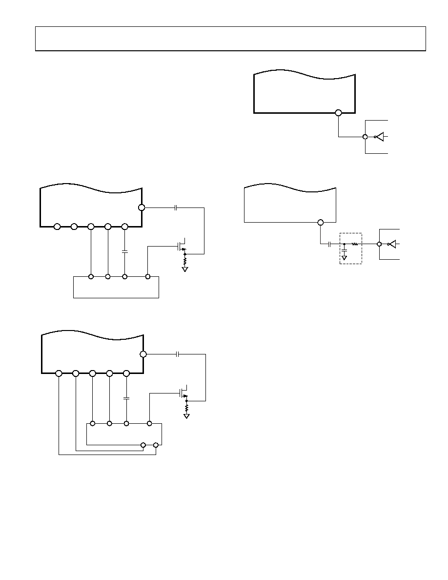
DRIVING THE CLI INPUT
The AD9949’s master clock input (CLI) may be used in two
different configurations, depending on the application.
Figure 41 shows a typical dc-coupled input from the master
clock source. When the dc-coupled technique is used, the
master clock signal should be at standard 3 V CMOS logic
levels. As shown in Figure 42, a 1000 pF ac-coupling capacitor
may be used between the clock source and the CLI input. In this
configuration, the CLI input is self-biased to the proper dc volt-
age level of approximately 1.4 V. When the ac-coupled tech-
nique is used, the master clock signal can be as low as ±500 mV
in amplitude.
CCD IMAGER
SIGNAL
OUT
H2
RG
H3
H4
H1
H2
H1
RG
AD9949
CCDIN
03751-040
18
19
14
15
21
27
Figure 39. CCD Connections (2 H-Clock)
03751-041
CCD IMAGER
SIGNAL
OUT
H4
RG
H1
H2
H3
H4
H2
H1
H3
RG
AD9949
CCDIN
14
15
18
19
21
27
Figure 40. CCD Connections (4 H-Clock)
03751-042
CLI
AD9949
25
ASIC
MASTER CLOCK
Figure 41. CLI Connection, DC-Coupled
LPF
1nF
03751-
043
CLI
AD9949
25
ASIC
MASTER CLOCK
Figure 42. CLI Connection, AC-Coupled
HORIZONTAL TIMING SEQUENCE EXAMPLE
Figure 43 shows an example CCD layout. The horizontal
register contains 28 dummy pixels, which occur on each line
clocked from the CCD. In the vertical direction, there are
10 optical black (OB) lines at the front of the readout and two at
the back of the readout. The horizontal direction has four OB
pixels in the front and 48 in the back.
To configure the AD9949 horizontal signals for this CCD, three
sequences can be used. Figure 44 shows the first sequence that
should be used during vertical blanking. During this time, there
are no valid OB pixels from the sensor, so the CLPOB signal is
not used. PBLK may be enabled during this time, because no
valid data is available.
Figure 45 shows the recommended sequence for the vertical OB
interval. The clamp signals are used across the whole lines in
order to stabilize the clamp loop of the AD9949.
Figure 46 shows the recommended sequence for the effective
pixel readout. The 48 OB pixels at the end of each line are used
for the CLPOB signal.
相关PDF资料 |
PDF描述 |
|---|---|
| 2081204-9 | CONN JACK SMA BULKHEAD RG405 |
| AD9949KCPZRL | IC CCD SIGNAL PROCESSOR 40-LFCSP |
| 2081204-7 | CONN JACK SMA BULKHEAD RG58 |
| 2081204-5 | CONN JACK SMA BULKHEAD RD316 |
| AD9948KCPZRL | IC CCD SIGNAL PROCESSOR 40-LFCSP |
相关代理商/技术参数 |
参数描述 |
|---|---|
| AD9949BCBZRL | 制造商:Analog Devices 功能描述: |
| AD9949KCP | 制造商:Analog Devices 功能描述:AFE Video 1ADC 12-Bit 3V 40-Pin LFCSP EP 制造商:Rochester Electronics LLC 功能描述:12 BIT 36 MSPS, 3 V ANALOG FRONT END - Bulk |
| AD9949KCPRL | 制造商:Analog Devices 功能描述:AFE Video 1ADC 12-Bit 3V 40-Pin LFCSP EP T/R 制造商:Rochester Electronics LLC 功能描述:12 BIT 36 MSPS, 3 V ANALOG FRONT END - Tape and Reel |
| AD9949KCPZ | 功能描述:IC CCD SIGNAL PROCESSOR 40-LFCSP RoHS:是 类别:集成电路 (IC) >> 接口 - 传感器和探测器接口 系列:- 其它有关文件:Automotive Product Guide 产品培训模块:Lead (SnPb) Finish for COTS Obsolescence Mitigation Program 标准包装:74 系列:- 类型:触控式传感器 输入类型:数字 输出类型:数字 接口:JTAG,串行 电流 - 电源:100µA 安装类型:表面贴装 封装/外壳:20-TSSOP(0.173",4.40mm 宽) 供应商设备封装:20-TSSOP 包装:管件 |
| AD9949KCPZRL | 功能描述:IC CCD SIGNAL PROCESSOR 40-LFCSP RoHS:是 类别:集成电路 (IC) >> 接口 - 传感器和探测器接口 系列:- 其它有关文件:Automotive Product Guide 产品培训模块:Lead (SnPb) Finish for COTS Obsolescence Mitigation Program 标准包装:74 系列:- 类型:触控式传感器 输入类型:数字 输出类型:数字 接口:JTAG,串行 电流 - 电源:100µA 安装类型:表面贴装 封装/外壳:20-TSSOP(0.173",4.40mm 宽) 供应商设备封装:20-TSSOP 包装:管件 |
发布紧急采购,3分钟左右您将得到回复。