- 您现在的位置:买卖IC网 > PDF目录10979 > AD9952YSVZ (Analog Devices Inc)IC DDS 14BIT DAC 1.8V 48-TQFP PDF资料下载
参数资料
| 型号: | AD9952YSVZ |
| 厂商: | Analog Devices Inc |
| 文件页数: | 15/28页 |
| 文件大小: | 0K |
| 描述: | IC DDS 14BIT DAC 1.8V 48-TQFP |
| 产品培训模块: | Direct Digital Synthesis Tutorial Series (1 of 7): Introduction Direct Digital Synthesizer Tutorial Series (7 of 7): DDS in Action Direct Digital Synthesis Tutorial Series (3 of 7): Angle to Amplitude Converter Direct Digital Synthesis Tutorial Series (6 of 7): SINC Envelope Correction Direct Digital Synthesis Tutorial Series (4 of 7): Digital-to-Analog Converter Direct Digital Synthesis Tutorial Series (2 of 7): The Accumulator |
| 标准包装: | 1 |
| 分辨率(位): | 14 b |
| 主 fclk: | 400MHz |
| 调节字宽(位): | 32 b |
| 电源电压: | 1.71 V ~ 1.96 V |
| 工作温度: | -40°C ~ 105°C |
| 安装类型: | 表面贴装 |
| 封装/外壳: | 48-TQFP 裸露焊盘 |
| 供应商设备封装: | 48-TQFP 裸露焊盘(7x7) |
| 包装: | 托盘 |
| 产品目录页面: | 552 (CN2011-ZH PDF) |
第1页第2页第3页第4页第5页第6页第7页第8页第9页第10页第11页第12页第13页第14页当前第15页第16页第17页第18页第19页第20页第21页第22页第23页第24页第25页第26页第27页第28页
AD9952
Rev. B | Page 22 of 28
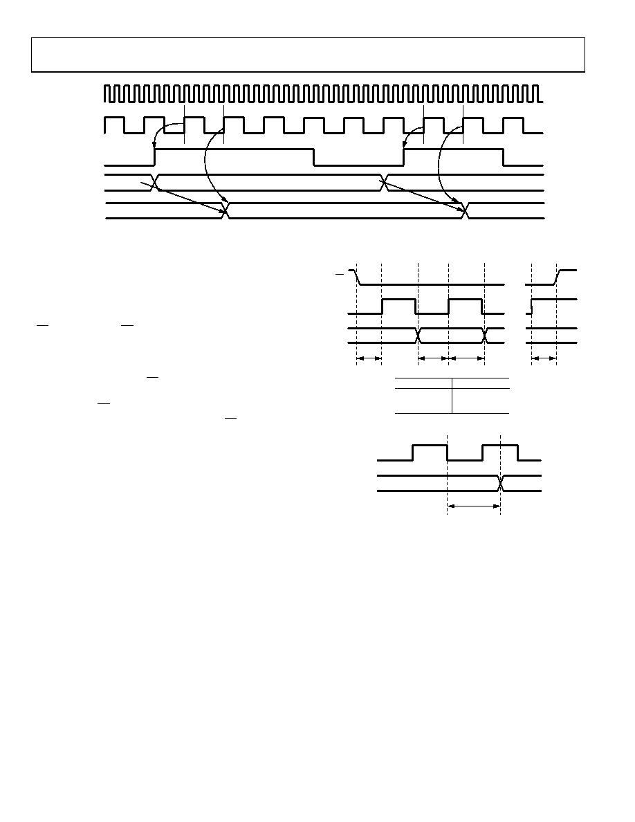
SYSCLK
SYNC_CLK
I/O UPDATE
DATA IN
I/O BUFFERS
DATA IN
REGISTERS
AB
DATA 1
DATA 2
DATA 3
DATA 0
DATA 1
DATA 2
THE DEVICE REGISTERS AN I/O UPDATE AT POINT A. THE DATA IS TRANSFERRED FROM THE I/O BUFFERS AT POINT B.
03
35
8-
0
31
Figure 26. Timing of I/O Update Signal vs. Actual Register Update
Serial Interface Port Pin Description
SCLK—Serial Clock. The serial clock pin is used to synchronize
data to and from the AD9952 and to run the internal state
machines. SCLK maximum frequency is 25 MHz.
CS—Chip Select Bar. CS is active low input that allows more
than one device on the same serial communication line. The
SDO pin and SDIO pin go to a high impedance state when this
input is high. If driven high during any communication cycle,
the cycle is suspended until CS is reactivated low. Chip select
can be tied low in systems that maintain control of SCLK.
When toggling CS, it is important that care is taken to meet the
clock setup time with respect to the falling edge of CS and TCSU
(see Figure 27).
SDIO—Serial Data I/O. Data is always written into the AD9952
on this pin. However, this pin can be used as a bidirectional
data line. Bit 9 of Register 0x00 controls the configuration of
this pin. The default is Logic 0, which configures the SDIO pin
as bidirectional. In order to guarantee proper serial I/O port
operation (see Figure 27), data on this pin must be set up and held
to the rising edge of SCLK on read operations.
SDO—Serial Data Out. Data is read from this pin for protocols
that use separate lines for transmitting and receiving data. In
the case where the AD9952 operates in a single bidirectional
I/O mode, this pin does not output data and is set to a high
impedance state.
IOSYNC—Synchronizes the I/O port state machines without
affecting the registers’ contents. An active high input on the
IOSYNC pin causes the current communication cycle to abort.
After IOSYNC returns low (Logic 0), another communication
cycle can begin, starting with the instruction byte write.
● ● ●
SCLK
SDIO
CS
TCSU
TDSU
TDH
DVDD I/O = 3.3V
TCSU = 3ns
TDSU = 3ns
TDH = 0ns
DVDD I/O = 1.8V
TCSU = 5ns
TDSU = 5ns
TDH = 0ns
03
35
8-
0
32
Figure 27. Serial Port I/O Setup (TCSU, TDSU) and Hold (TDH) Times
TDV = 25ns
SCLK
SDIO
SDO
03
35
8-
03
3
Figure 28. Serial Port I/O Data Valid Time (TDV) During Readback
MSB/LSB Transfers
The AD9952 serial port can support both most significant bit
(MSB) first or least significant bit (LSB) first data formats. The
control register, Register 0x00, Bit 8, controls this functionality.
The default value of Register 0x00 [8] is low (MSB first).
When the control register (0x00 [8]) is set high, the AD9952
serial port is in LSB-first format. The instruction byte must be
written in the format indicated by the control register (0x00
[8]), and the instruction byte must be written from least
significant bit to most significant bit (right to left in the table
located in the Instruction Byte Details section).
Note that even in LSB-first mode, the two respective phases of
the communication cycle, the instruction byte phase and the
data communication phase, retain their respective positions.
相关PDF资料 |
PDF描述 |
|---|---|
| MC9S08DZ96MLF | MCU 8BIT 96K FLASH 48-LQFP |
| AD5933YRSZ | IC NTWK ANALYZER 12B 1MSP 16SSOP |
| MC908JL3EMPE | IC MCU 4K FLASH W/OSC 28-PDIP |
| MC908AP8CFAE | IC MCU 8K FLASH 8MHZ 48-LQFP |
| AD9851BRSZ | IC SYNTHESIZER DDS/DAC 28-SSOP |
相关代理商/技术参数 |
参数描述 |
|---|---|
| AD9952YSVZ | 制造商:Analog Devices 功能描述:IC DDS 400MSPS SMD 9952 TQFP48 |
| AD9952YSVZ-REEL7 | 功能描述:IC DDS DAC 14BIT 1.8V 48TQFP RoHS:是 类别:集成电路 (IC) >> 接口 - 直接数字合成 (DDS) 系列:- 产品变化通告:Product Discontinuance 27/Oct/2011 标准包装:2,500 系列:- 分辨率(位):10 b 主 fclk:25MHz 调节字宽(位):32 b 电源电压:2.97 V ~ 5.5 V 工作温度:-40°C ~ 85°C 安装类型:表面贴装 封装/外壳:16-TSSOP(0.173",4.40mm 宽) 供应商设备封装:16-TSSOP 包装:带卷 (TR) |
| AD9953 | 制造商:AD 制造商全称:Analog Devices 功能描述:400 MSPS 14-Bit, 1.8V CMOS Direct Digital Synthesizer |
| AD9953/PCB | 制造商:Analog Devices 功能描述:400 MSPS, 14BIT DGTL SYNTHESIZER - Bulk |
| AD9953ASV | 制造商:AD 制造商全称:Analog Devices 功能描述:400 MSPS 14-Bit, 1.8V CMOS Direct Digital Synthesizer |
发布紧急采购,3分钟左右您将得到回复。