- 您现在的位置:买卖IC网 > PDF目录2063 > ADA4859-3ACPZ-RL (Analog Devices Inc)IC AMP 3CH CFB G=2 W/CP 16LFCSP PDF资料下载
参数资料
| 型号: | ADA4859-3ACPZ-RL |
| 厂商: | Analog Devices Inc |
| 文件页数: | 4/16页 |
| 文件大小: | 0K |
| 描述: | IC AMP 3CH CFB G=2 W/CP 16LFCSP |
| 标准包装: | 5,000 |
| 应用: | 电流反馈 |
| 电路数: | 3 |
| -3db带宽: | 265MHz |
| 转换速率: | 740 V/µs |
| 电流 - 电源: | 17mA |
| 电流 - 输出 / 通道: | 19mA |
| 电压 - 电源,单路/双路(±): | 3 V ~ 5.5 V |
| 安装类型: | 表面贴装 |
| 封装/外壳: | 16-VQFN 裸露焊盘,CSP |
| 供应商设备封装: | 16-LFCSP-VQ EP(4x4) |
| 包装: | 带卷 (TR) |
ADA4859-3
Data Sheet
Rev. A | Page 12 of 16
THEORY OF OPERATION
OVERVIEW
The ADA4859-3 is a fixed gain of two, current feedback amplifier
designed for exceptional performance as a triple video amplifier. Its
specifications make it especially suitable for SD and HD video
applications. The ADA4859-3 provides HD video output on a
single supply as low as 3.0 V while only consuming 13 mA per
amplifier. It also features a power-down pin (PD) that reduces
the quiescent current to 4 mA when activated.
The ADA4859-3 can be used in applications that require both
ac- and dc-coupled inputs and outputs. The output stage on the
ADA4859-3 is capable of driving 2 V p-p video signals into two
doubly terminated video loads (150 each) on a single 5 V supply.
The input range of the ADA4859-3 includes ground, whereas
the output range is limited by the output headroom set by the
voltage drop across two diodes from each rail, which occurs
1.2 V from the positive and negative supply rails.
CHARGE PUMP OPERATION
The on-board charge pump creates a negative supply for the
amplifier. It provides different negative voltages depending on
the power supply voltage. For a +5 V supply, the negative supply
generated is equal to 3 V with 150 mA of output supply current,
and for a +3.3 V supply, the negative supply is equal to 2 V
with 45 mA of output supply current.
charges C1 through Φ1 to ground. During this cycle, C1 quickly
charges to reach the +VS voltage. The discharge cycle then begins
When C1 = C2, the charge in C1 is divided between the two
capacitors and slowly increases the voltage in C2 until it reaches a
predetermined voltage (3 V for the +5 V supply and 2 V for
the +3.3 V supply). The typical charge pump charging and
discharging frequency is 550 kHz with a 150 load and no input
signal. This frequency changes with the load current, and it can
get much slower if the amplifier is powered down and no external
current is used.
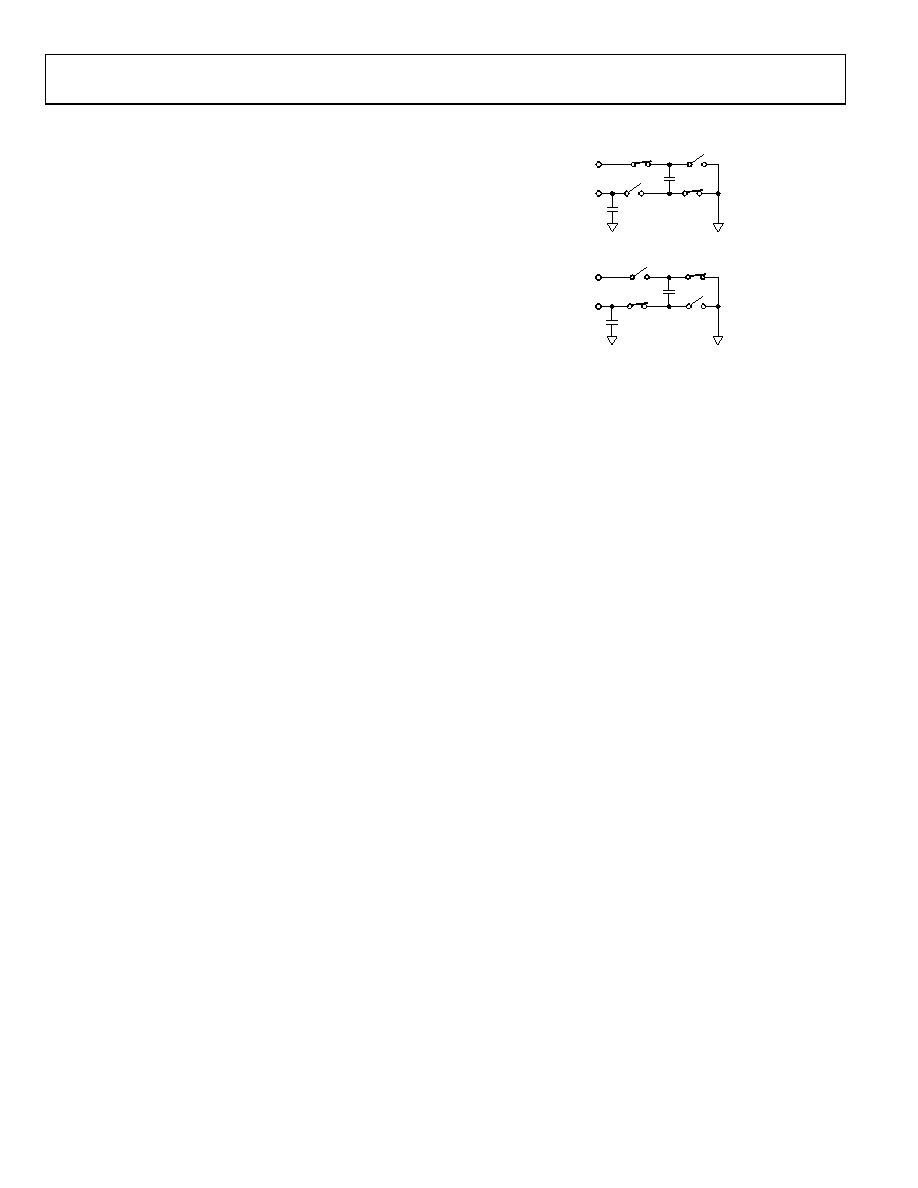
07715-
137
+VS
CPO
C2
C1
Φ1
a
b
Figure 30. Charging Cycle
07715-
138
+VS
CPO
C2
C1
Φ2
a
b
Figure 31. Discharging Cycle
The ADA4859-3 specifications make it especially suitable for SD
and HD video applications. It also allows dc-coupled video signal
with its black level set to 0 V and its sync tip down to 300 mV
for YPbPr video.
The charge pump is always on, even when the power-down pin
(PD) is enabled and the amplifier is off. However, it would be in
an idle state if the negative current were not used. Each amplifier
needs 6.3 mA of current, which totals 19 mA for all three
amplifiers. This means additional negative current may be available
by the charge pump for external use. Pin 4 (CPO) is the charge
pump output, which provides access to the negative supply
generated by the charge pump. Placing a 1 F charge capacitor at
the CPO pin is essential to hold the charge and regulate the ripple.
If the negative supply is used to power another device in the
system, it is only possible for the 5 V supply operation. In the
3.3 V supply operation, the charge pump output current is very
limited. The capacitor at the CPO pin, which regulates the ripple
of the negative voltage, can be used as a coupling capacitor for the
external device. However, the charge pump current should be
limited to a maximum of 50 mA for external use. When powering
down the ADA4859-3, the charge pump is not affected and its
output voltage and current remain available for external use.
相关PDF资料 |
PDF描述 |
|---|---|
| ADA4922-1ACPZ-R2 | IC ADC DRIVER 18BIT DIFF 8-LFCSP |
| ADA4937-2YCPZ-RL | IC ADC DRIVER DUAL DIFF 24LFCSP |
| ADA4938-2ACPZ-RL | IC ADC DRIVER DUAL DIFF 24LFCSP |
| ADA4941-1YRZ-R7 | IC DIFF ADC DRIVER 18BIT 8SOIC |
| ADA4960-1ACPZ-R2 | IC ADC DRIVER DIFF 16LFCSP |
相关代理商/技术参数 |
参数描述 |
|---|---|
| ADA4860-1 | 制造商:AD 制造商全称:Analog Devices 功能描述:High Speed, Low Cost, Op Amp |
| ADA4860-1YRJ-EBZ | 功能描述:BOARD EVAL FOR ADA4860-1YRJ RoHS:是 类别:编程器,开发系统 >> 评估板 - 运算放大器 系列:- 产品培训模块:Lead (SnPb) Finish for COTS Obsolescence Mitigation Program 标准包装:1 系列:- |
| ADA4860-1YRJZ-R2 | 制造商:Analog Devices 功能描述:OP Amp Single Current Fdbk 制造商:Analog Devices 功能描述:OP AMP SGL CURRENT FDBK 12V 6PIN SOT-23 - Tape and Reel 制造商:Analog Devices 功能描述:ANAADA4860-1YRJZ-R2 LOW COST CURRENT FEE |
| ADA4860-1YRJZ-RL | 功能描述:IC OPAMP CF LP 85MA SOT23-6 RoHS:是 类别:集成电路 (IC) >> Linear - Amplifiers - Instrumentation 系列:- 标准包装:160 系列:- 放大器类型:通用 电路数:4 输出类型:满摆幅 转换速率:10 V/µs 增益带宽积:9MHz -3db带宽:- 电流 - 输入偏压:1pA 电压 - 输入偏移:250µV 电流 - 电源:730µA 电流 - 输出 / 通道:28mA 电压 - 电源,单路/双路(±):2.7 V ~ 5.5 V,±1.35 V ~ 2.75 V 工作温度:-40°C ~ 125°C 安装类型:表面贴装 封装/外壳:16-SOIC(0.154",3.90mm 宽) 供应商设备封装:16-SOIC N 包装:管件 |
| ADA4860-1YRJZ-RL7 | 功能描述:IC OPAMP CF LP 85MA SOT23-6 RoHS:是 类别:集成电路 (IC) >> Linear - Amplifiers - Instrumentation 系列:- 产品培训模块:Differential Circuit Design Techniques for Communication Applications 标准包装:1 系列:- 放大器类型:RF/IF 差分 电路数:1 输出类型:差分 转换速率:9800 V/µs 增益带宽积:- -3db带宽:2.9GHz 电流 - 输入偏压:3µA 电压 - 输入偏移:- 电流 - 电源:40mA 电流 - 输出 / 通道:- 电压 - 电源,单路/双路(±):3 V ~ 3.6 V 工作温度:-40°C ~ 85°C 安装类型:表面贴装 封装/外壳:16-VQFN 裸露焊盘,CSP 供应商设备封装:16-LFCSP-VQ 包装:剪切带 (CT) 产品目录页面:551 (CN2011-ZH PDF) 其它名称:ADL5561ACPZ-R7CT |
发布紧急采购,3分钟左右您将得到回复。